Rainbow Electronics MAX9792 User Manual
Page 24
MAX9791/MAX9792
Windows Vista-Compliant Class D Speaker
Amplifiers with DirectDrive Headphone Amplifiers
24
______________________________________________________________________________________
Component Selection
Speaker Amplifier Power-Supply Input (PVDD)
PVDD powers the speaker amplifiers. PVDD ranges
from 4.5V to 5.5V. Bypass PVDD with a 0.1µF capacitor
to PGND. Apply additional bulk capacitance at the
device if long input traces between PVDD and the
power source are used.
Headphone Amplifier Power-Supply Input
(HPVDD and CPVSS)
The headphone amplifiers are powered from HPVDD
and CPVSS. HPVDD is the positive supply of the head-
phone amplifiers and ranges from 2.7V to 5.5V. Bypass
HPVDD with a 10µF capacitor to PGND. CPVSS is the
negative supply of the headphone amplifiers. Bypass
CPVSS with a 1µF capacitor to PGND. The charge
pump inverts the voltage at HPVDD, and the resulting
voltage appears at CPVSS. A 1µF capacitor should be
connected between C1N and C1P.
Positive Power Supply and LDO Input (AVDD)
The internal LDO and the remainder of the device are
powered by AVDD. AVDD ranges from 4.5V to 5.5V.
Bypass AVDD with a 0.1µF capacitor to GND and two
1µF capacitors to GND. Note additional bulk capaci-
tance is required at the device if long input traces
between AVDD and the power source are used.
Input Filtering
The input capacitor (C
IN_
), in conjunction with the
amplifier input resistance (R
IN_
), forms a highpass filter
that removes the DC bias from the incoming signal.
The AC-coupling capacitor allows the amplifier to bias
the signal to an optimum DC level. Assuming zero
source impedance, the -3dB point of the highpass filter
is given by:
R
IN_
is the amplifier’s external input resistance value.
Choose C
IN_
such that f
-3dB
is well below the lowest fre-
quency of interest. Setting f
-3dB
too high affects the ampli-
fier’s low frequency response. Use capacitors with
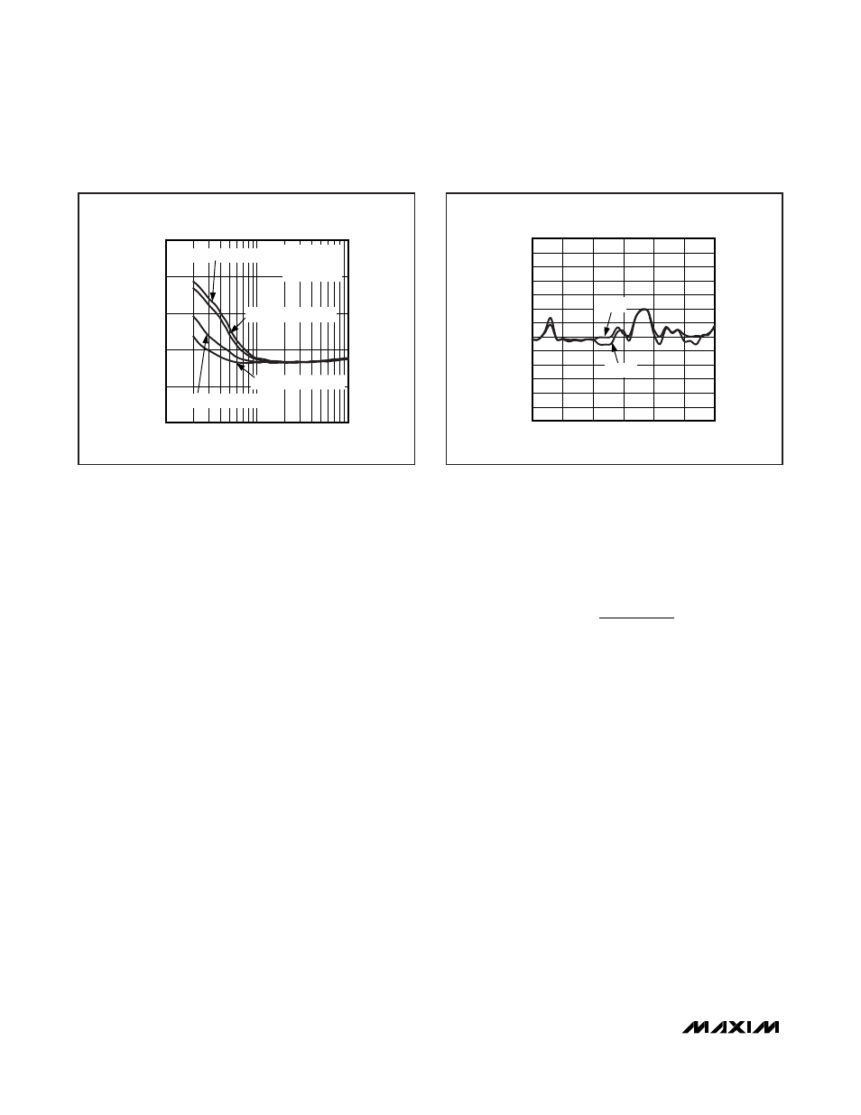
adequately low-voltage coefficient dielectrics (see Figure
12). Capacitors with higher voltage coefficients, such as
ceramics, result in increased distortion at low frequencies.
Charge-Pump Capacitor Selection
Use capacitors with an ESR less than 100m
Ω for opti-
mum performance. Low ESR ceramic capacitors mini-
mize the output resistance of the charge pump. For
best performance over the extended temperature
range, select capacitors with an X7R dielectric.
Flying Capacitor (C1)
The value of the flying capacitor (C1) affects the load
regulation and output resistance of the charge pump. A
C1 value that is too small degrades the device’s ability
to provide sufficient current drive, which leads to a loss
of output voltage. Connect a 1µF capacitor between
C1P and C1N.
f
R
C
dB
IN
IN
-3
1
2
=
π
_
_
INPUT COUPLING CAPACITOR-INDUCED THD+N
vs. FREQUENCY (HEADPHONE MODE)
FREQUENCY (kHz)
THD+N (dBFS)
100
-90
-80
-70
-60
-50
-100
10
1000
0603 10V X5R 10% 1
μF
0603 10V X7R 10% 1
μF
0402 6.3V X5R 10% 1
μF
0805 50V X7R 10% 1
μF
V
OUT
- -3dBFS
FS = 1V
RMS
R
L
=32
Ω
Figure 12. Input Coupling Capacitor-Induced THD+N vs.
Frequency
SPEAKER RF IMMUNITY
vs. FREQUENCY
FREQUENCY (MHz)
AMPLITUDE (dBV)
2500
2000
1500
1000
500
-120
-110
-100
-90
-80
-70
-60
-50
-40
-30
-20
-10
0
-130
0
3000
RIGHT
LEFT
Figure 13. Speaker RF Immunity