Rainbow Electronics MAX9792 User Manual
Page 2
MAX9791/MAX9792
Windows Vista-Compliant Class D Speaker
Amplifiers with DirectDrive Headphone Amplifiers
2
_______________________________________________________________________________________
ABSOLUTE MAXIMUM RATINGS
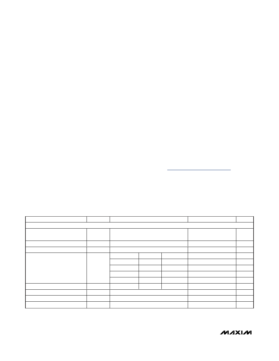
ELECTRICAL CHARACTERISTICS
(V
AVDD
= V
PVDD
= V
HPVDD
= 5V, V
GND
= V
PGND
= V
CPGND
= 0, I
LDO_OUT
= 0, C
LDO
= 2µF, C1 = C2 = 1µF. R
L
=
∞, unless other-
wise specified. R
IN1
= 20k
Ω (A
VSPKR
= 12dB), R
IN2
= 40.2k
Ω (A
VHP
= 0dB), C
IN1
= 470nF, C
IN2
= C
COM
= 1µF, T
A
= T
MIN
to T
MAX
,
unless otherwise noted. Typical values are at T
A
= +25°C.) (Note 3)
Stresses beyond those listed under “Absolute Maximum Ratings” may cause permanent damage to the device. These are stress ratings only, and functional
operation of the device at these or any other conditions beyond those indicated in the operational sections of the specifications is not implied. Exposure to
absolute maximum rating conditions for extended periods may affect device reliability.
Supply Voltage
(AVDD, PVDD, HPVDD to GND)........................-0.3V to +6.0V
GND to PGND, CPGND ......................................................±0.3V
CPVSS, C1N to GND ............................................-6.0V to + 0.3V
HPL, HPR to CPVSS ...........................................-0.3V to lower of
(HPVDD - CPVSS + 0.3V) and +9V
HPL, HPR to HPVDD..................................+0.3V to the higher of
(CPVSS - HPVDD - 0.3V) and -9V
COM, SENSE........................................................-0.3V to + 0.3V
Any Other Pin ..........................................-0.3V to (AVDD + 0.3V)
Duration of Short Circuit between OUT_+, OUT_- and GND,
PGND, AVDD, or PVDD..........................................Continuous
Duration of Short Circuit between LDO_OUT and AVDD,
GND (Note 1) .........................................................Continuous
Duration of Short Circuit between HPR, HPL and
GND .......................................................................Continuous
Continuous Current (PVDD, OUT_+, OUT_-, PGND)............1.7A
Continuous Current (C1N, C1P, CPVSS, AVDD, HPVDD,
LDO_OUT, HPR, HPL) ..................................................850mA
Continuous Input Current (All Other Pins) ........................±20mA
Continuous Power Dissipation (T
A
= +70°C)
28-Pin Thin QFN Single-Layer Board (derate 20.8mW/°C
above +70°C)..........................................................1667mW
Junction-to-Ambient Thermal Resistance (
θ
JA
)
(Note 2) .....................................................................40°C/W
Junction-to-Case Thermal Resistance (
θ
JC
)
(Note 2) ....................................................................2.7°C/W
28-Pin Thin QFN Multilayer Board (derate 28.6mW/°C
above +70°C)..........................................................2286mW
Junction-to-Ambient Thermal Resistance (
θ
JA
)
(Note 2) .....................................................................35°C/W
Junction-to-Case Thermal Resistance (
θ
JC
)
(Note 2) ....................................................................2.7°C/W
ESD Protection, Human Body Model ...................................±2kV
Operating Temperature Range ...........................-40°C to +85°C
Junction Temperature ......................................................+150°C
Storage Temperature Range .............................-65°C to +150°C
Lead Temperature (soldering, 10s) .................................+300°C
PARAMETER
SYMBOL
CONDITIONS
MIN
TYP
MAX
UNITS
GENERAL
Supply Voltage
V
AVDD
,
V
PVDD
Guaranteed by PSRR test
4.5
5.5
V
Headphone Supply Voltage
V
HPVDD
Guaranteed by PSRR test
2.7
5.5
V
Undervoltage Lockout
UVLO
2.65
V
SPKR_EN
HP_EN
LDO_EN
1
0
1
250
400
µA
1
1
0
4.4
6
mA
0
0
0
10.5
15
mA
Quiescent Current
I
AVDD
+
I
PVDD
+
I
HPVDD
0
1
0
14.4
21
mA
Shutdown Current
I
SHDN
1
0
0
0.1
1
µA
Bias Voltage
V
BIAS
HP_INR, HP_INL, SPKR_INR, SPKR_INL
0
V
Shutdown to Full Operation
t
ON
0.4
ms
Overtemperature Threshold
+150
°C
Note 1: If short is present at power-up.
Note 2: Package thermal resistances were obtained using the method described in JEDEC specification JESD51-7, using a four-layer