Absolute maximum ratings, Electrical characteristics – Rainbow Electronics MAX6636 User Manual
Page 2
MAX6636
7-Channel Precision Temperature Monitor
2
_______________________________________________________________________________________
ABSOLUTE MAXIMUM RATINGS
Stresses beyond those listed under “Absolute Maximum Ratings” may cause permanent damage to the device. These are stress ratings only, and functional
operation of the device at these or any other conditions beyond those indicated in the operational sections of the specifications is not implied. Exposure to
absolute maximum rating conditions for extended periods may affect device reliability.
V
CC
, SCK, SDA,
ALERT, OVERT, STBY to GND ......-0.3V to +6V
DXP_ to GND..............................................-0.3V to (V
CC
+ 0.3V)
DXN2, DXN3, DXN4, DXN5, DXN6 to GND...........-0.3V to +0.8V
SDA,
ALERT, OVERT Current .............................-1mA to +50mA
DXN Current .......................................................................±1mA
Continuous Power Dissipation (T
A
= +70°C)
20-Pin TSSOP
(derate 11.0mW/°C above +70°C)..............................879.1mW
Junction-to-Case Thermal Resistance (
θ
JC
) (Note A)
20-Pin TSSOP...............................................................20°C/W
Junction-to-Ambient Thermal Resistance (
θ
JA
) (Note A)
20-Pin TSSOP............................................................73.8°C/W
ESD Protection (all pins, Human Body Model) ................±2000V
Operating Temperature Range .........................-40°C to +125°C
Junction Temperature ......................................................+150°C
Storage Temperature Range .............................-60°C to +150°C
Lead Temperature (soldering, 10s) .................................+300°C
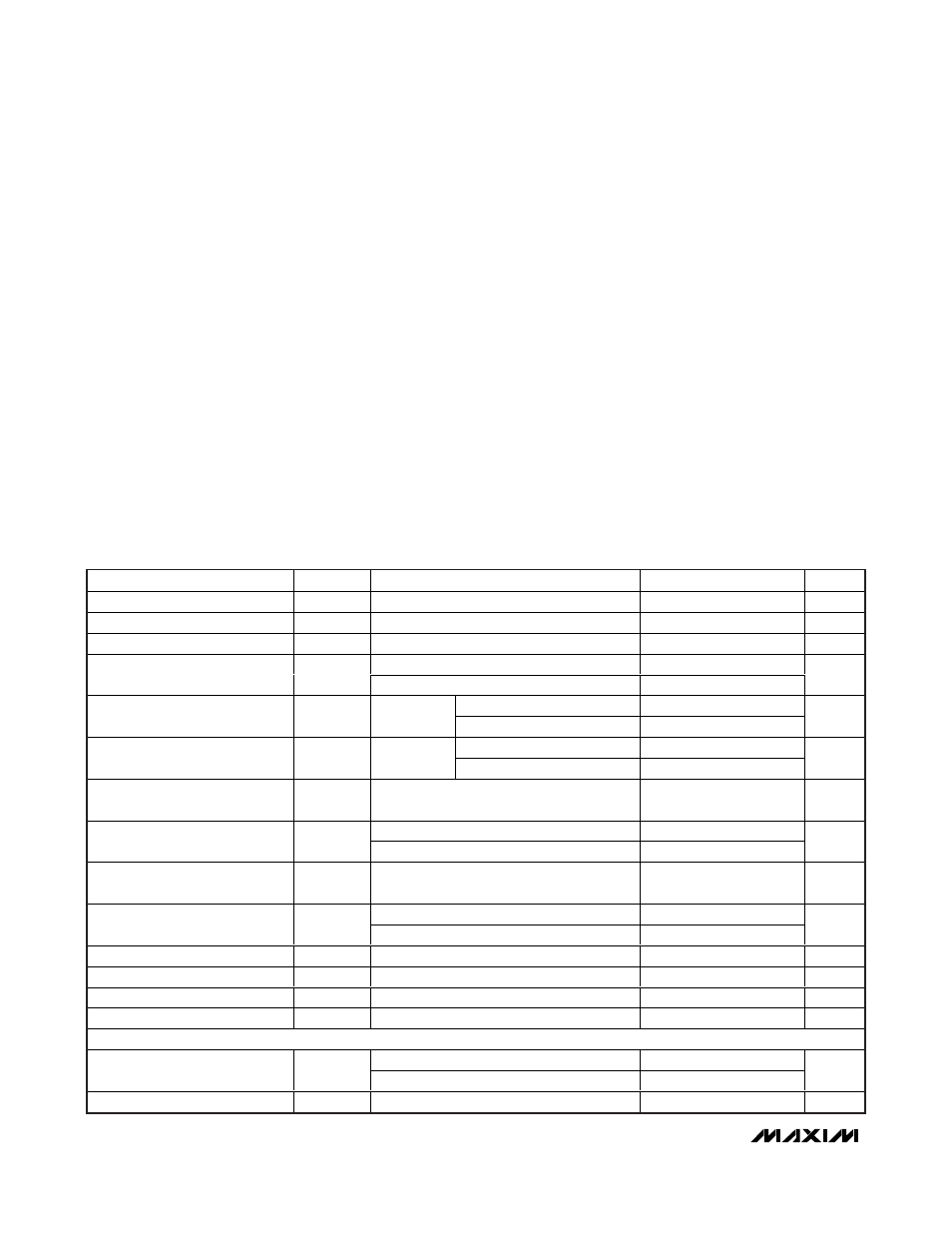
ELECTRICAL CHARACTERISTICS
(V
CC
= +3.0V to +5.5V, V
STBY
= V
CC
, T
A
= -40°C to +125°C, unless otherwise noted. Typical values are at V
CC
= +3.3V and
T
A
= +25°C.) (Note 1)
PARAMETER
SYMBOL
CONDITIONS
MIN
TYP
MAX
UNITS
Supply Voltage
V
CC
3.0
5.5
V
Software Standby Supply Current
I
SS
SMBus static
30
µA
Operating Current
I
CC
During conversion
500
1000
µA
Channel 1 only
11
Temperature Resolution
Other diode channels
8
Bits
T
A
= T
RJ
= +60°C to +100°C
-1.0
+1.0
Remote Temperature Accuracy
V
CC
= 3.3V
T
A
= T
RJ
= 0°C to +125°C
-3.0
+3.0
o
C
T
A
= +60°C to +100°C
-4.4
-0.4
Local Temperature Accuracy
V
CC
= 3.3V
T
A
= 0°C to +125°C
-6.1
-0.1
o
C
Supply Sensitivity of Temperature
Accuracy
±0.2
o
C/V
Resistance cancellation off
95
125
156
Remote Channel 1 Conversion
Time
t
CONV1
Resistance cancellation on
190
250
312
ms
Remote Channels 2 Through 6
Conversion Time
t
CONV_
95
125
156
ms
High level
80
100
120
Remote-Diode Source Current
I
RJ
Low level
8
10
12
µA
Undervoltage-Lockout Threshold
UVLO
Falling edge of V
CC
disables ADC
2.30
2.80
2.95
V
Undervoltage-Lockout Hysteresis
90
mV
Power-On-Reset (POR) Threshold
V
CC
falling edge
1.2
2.0
2.5
V
POR Threshold Hysteresis
90
mV
ALERT, OVERT
I
SINK
= 1mA
0.3
Output Low Voltage
V
OL
I
SINK
= 6mA
0.5
V
Output Leakage Current
1
µA
Note A: Package thermal resistances were obtained using the method described in JEDEC specification JESD51-7, using a 4-layer board.
For detailed information on package thermal considerations, refer to
Application Note 4083 at www.maxim-ic.com/thermal-tutorial.