Rainbow Electronics MAX16820 User Manual
Page 2
MAX16819/MAX16820
2MHz High-Brightness LED Drivers with
High-Side Current Sense and 5000:1 Dimming
2
_______________________________________________________________________________________
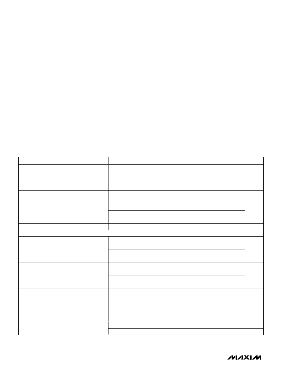
ABSOLUTE MAXIMUM RATINGS
ELECTRICAL CHARACTERISTICS
(V
IN
= 12V, V
DIM
= V
IN
, C
VCC
= 1µF, R
SENSE
= 0.5Ω, T
A
= T
J
= -40°C to +125°C, unless otherwise noted. Typical values are at
T
A
= +25°C.) (Note 1)
Stresses beyond those listed under “Absolute Maximum Ratings” may cause permanent damage to the device. These are stress ratings only, and functional
operation of the device at these or any other conditions beyond those indicated in the operational sections of the specifications is not implied. Exposure to
absolute maximum rating conditions for extended periods may affect device reliability.
IN, CSN, DIM to GND .............................................-0.3V to +30V
V
CC
, DRV to GND ....................................................-0.3V to +6V
CSN to IN...............................................................-0.3V to +0.3V
Maximum Current into Any Pin
(except IN, V
CC
, and DRV)............................................±20mA
Continuous Power Dissipation (T
A
= +70°C)
6-Pin TDFN (derate 18.17mW/
o
C
*
above +70°C).......1454mW
Operating Temperature Range .........................-40°C to +125°C
Junction Temperature ......................................................+150°C
Storage Temperature Range .............................-65°C to +150°C
Lead Temperature (soldering, 10s) .................................+300°C
Pin-to-Pin ESD Ratings (HB Model).....................................2.5kV
*As per JEDEC51 Standard (Single-Layer Board).
PARAMETER
SYMBOL
CONDITIONS
MIN
TYP
MAX
UNITS
Input Voltage Range
V
IN
4.5
28.0
V
Maximum Current Regulator
Switching Frequency
f
SW
2
MHz
Ground Current
I
GND
DRV open
1.5
mA
Supply Current
I
IN
V
DIM
< 0.6V
425
µA
V
IN
= V
CSN
= V
DIM
, V
IN
rising from 4V until
V
DRV
> V
CC
- 0.5V
4.7
5.0
Undervoltage Lockout
UVLO
V
IN
= V
CSN
= V
DIM
, V
IN
falling from 6V,
V
DRV
< 0.5V
4.5
V
Undervoltage Lockout Hysteresis
0.5
V
SENSE COMPARATOR
(V
IN
- V
CSN
) rising from 0V until V
DRV
<
0.5V (MAX16820)
195
210
225
Sense Voltage Threshold High
V
SNSHI
(V
IN
- V
CSN
) rising from 0V until V
DRV
<
0.5V (MAX16819)
213
230
246
mV
(V
IN
- V
CSN
) falling from 0.26V until V
DRV
>
(V
CC
- 0.5V) (MAX16820)
176
190
204
Sense Voltage Threshold Low
V
SNSLO
(V
IN
- V
CSN
) falling from 0.26V until V
DRV
>
(V
CC
- 0.5V) (MAX16819)
158
170
182
mV
Propagation Delay to Output
High
t
DPDH
Falling edge of (V
IN
- V
CSN
) from 0.26V to
0V to DRV high, C
DRV
= 1nF
82
ns
Propagation Delay to Output Low
t
DPDL
Rising edge of (V
IN
- V
CSN
) from 0V to
0.26V to DRV low, C
DRV
= 1nF
82
ns
Current-Sense Input Current
I
CSN
(V
IN
- V
CSN
) = 200mV
1
µA
MAX16819
56
70
mV
Current-Sense Threshold
Hysteresis
CS
HYS
MAX16820
17
35
mV