Ac electrical characteristics – Rainbow Electronics ADC12441 User Manual
Page 5
AC Electrical Characteristics
(Continued)
Note 4
The power dissipation of this device under normal operation should never exceed 169 mW (Quiescent Power Dissipation
a
TTL Loads on the digital
outputs) Caution should be taken not to exceed absolute maximum power rating when the device is operating in a severe fault condition (ex when any inputs or
outputs exceed the power supply) The maximum power dissipation must be derated at elevated temperatures and is dictated by T
Jmax
(maximum junction
temperature) i
JA
(package junction to ambient thermal resistance) and T
A
(ambient temperature) The maximum allowable power dissipation at any temperature
is P
Dmax
e
(T
Jmax
b
T
A
) i
JA
or the number given in the Absolute Maximum Ratings whichever is lower For this device T
Jmax
e
125 C and the typical thermal
resistance (i
JA
) of the ADC12441 with CMJ and CIJ suffixes when board mounted is 47 C W
Note 5
Human body model 100 pF discharged through a 1 5 kX resistor
Note 6
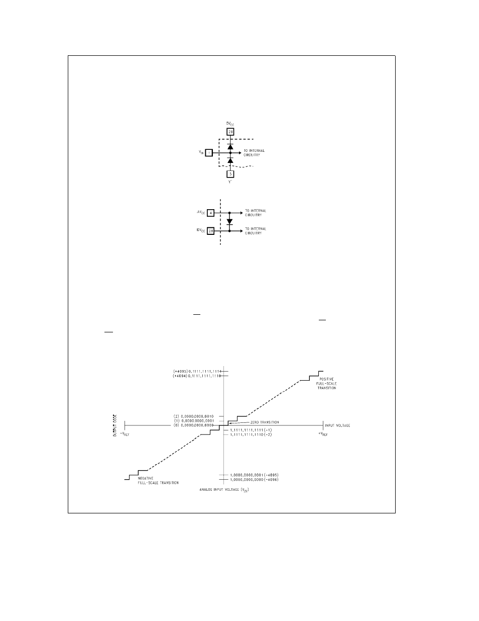
Two on-chip diodes are tied to the analog input as shown below Errors in the A D conversion can occur if these diodes are forward biased more than
50 mV
TL H 11017 – 3
This means that if AV
CC
and DV
CC
are minimum (4 75 V
DC
) and V
b
is maximum (
b
4 75 V
DC
) full-scale must be
s
4 8 V
DC
Note 7
A diode exists between AV
CC
and DV
CC
as shown below
TL H 11017 – 4
To guarantee accuracy it is required that the AV
CC
and DV
CC
be connected together to a power supply with separate bypass filters at each V
CC
pin
Note 8
Accuracy is guaranteed at f
CLK
e
2 0 MHz At higher and lower clock frequencies accuracy may degrade See curves in the Typical Performance
Characteristics section
Note 9
Typicals are at T
J
e
25 C and represent most likely parametric norm
Note 10
Limits are guaranteed to National’s AOQL (Average Outgoing Quality Level)
Note 11
Positive linearity error is defined as the deviation of the analog value expressed in LSBs from the straight line that passes through positive full scale and
zero For negative linearity error the straight line passes through negative full scale and zero (See
Figures 1b and 1c )
Note 12
The ADC12441’s self-calibration technique ensures linearity full scale and offset errors as specified but noise inherent in the self-calibration process will
result in a repeatability uncertainty of
g
0 20 LSB
Note 13
If T
A
changes then an Auto-Zero or Auto-Cal cycle will have to be re-started (see the Typical Performance Characteristic curves)
Note 14
After an Auto-Zero or Auto-Cal cycle at the specified power supply extremes
Note 15
If the clock is asynchronous to the falling edge of WR an uncertainty of one clock period will exist in the interval of t
A
therefore making the minimum
t
A
e
6 clock periods and the maximum t
A
e
7 clock periods If the falling edge of the clock is synchronous to the rising edge of WR then t
A
will be exactly 6 5 clock
periods
Note 16
The CAL line must be high before a conversion is started
Note 17
The specifications for these parameters are valid after an Auto-Cal cycle has been completed
Note 18
The ADC12441 reference ladder is composed solely of capacitors
Note 19
A Military RETS Electrical Test Specification is available on request At time of printing the ADC12441CMJ 883 RETS complies fully with the boldface
limits in this column
TL H 11017 – 5
FIGURE 1a Transfer Characteristic
5