Digital and dc electrical characteristics, Ac electrical characteristics – Rainbow Electronics ADC12441 User Manual
Page 4
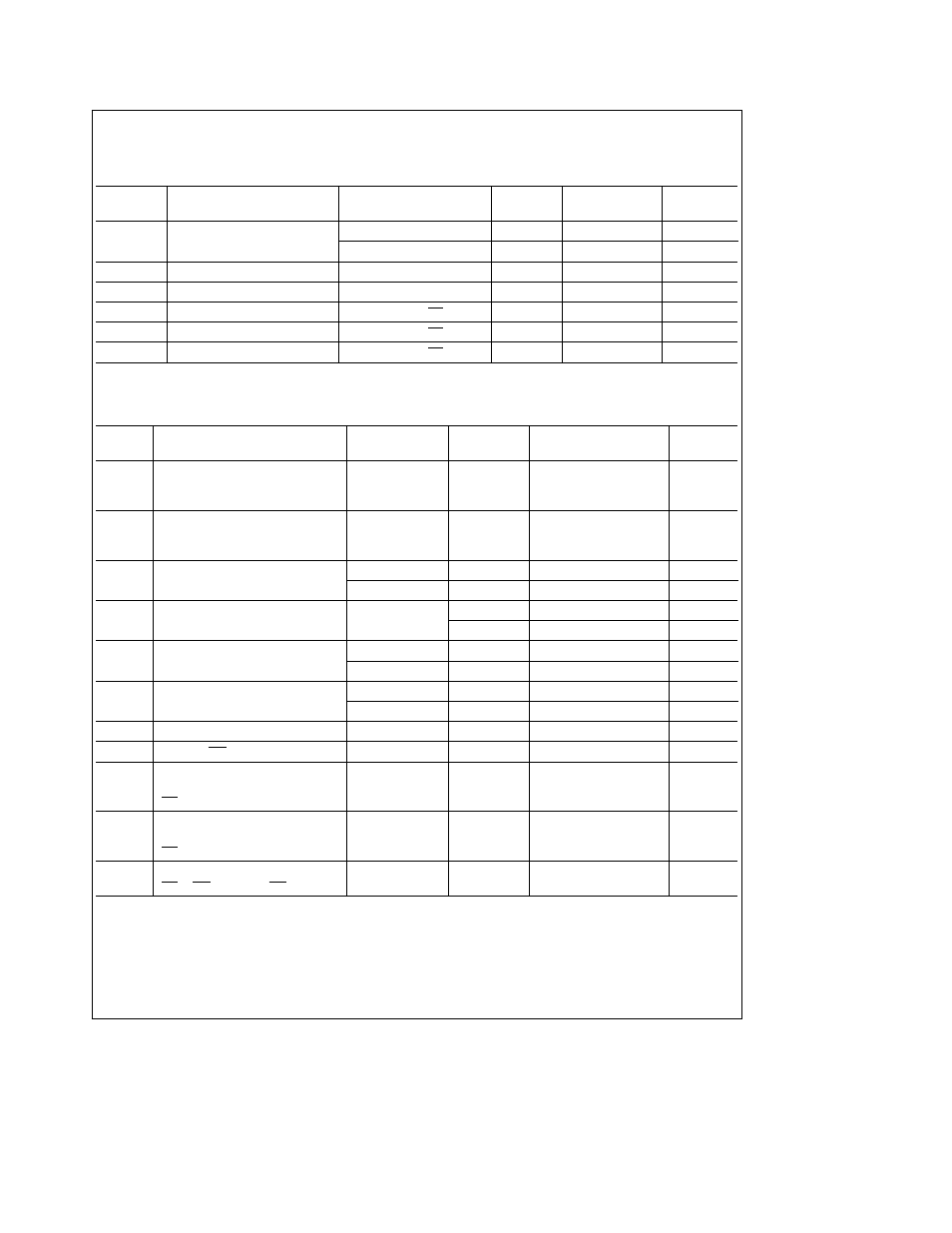
Digital and DC Electrical Characteristics
The following specifications apply for DV
CC
e
AV
CC
e a
5 0V V
b
e b
5 0V V
REF
e a
5 0V and f
CLK
e
2 0 MHz unless
otherwise specified Boldface limits apply for T
A
e
T
J
e
T
MIN
to T
MAX
all other limits T
A
e
T
J
e
25 C
(Notes 6 and 7) (Continued)
Symbol
Parameter
Conditions
Typical
Limit
Units
(Note 9)
(Notes 10 19)
(Limits)
I
OUT
TRI-STATE Output Leakage
V
OUT
e
0V
b
0 01
b
3
m
A (max)
Current
V
OUT
e
5V
0 01
3
m
A (max)
I
SOURCE
Output Source Current
V
OUT
e
0V
b
20
b
6 0
mA (min)
I
SINK
Output Sink Current
V
OUT
e
5V
20
8 0
mA (min)
DI
CC
DV
CC
Supply Current
f
CLK
e
2 MHz CS e ‘‘1’’
1
2
mA (max)
AI
CC
AV
CC
Supply Current
f
CLK
e
2 MHz CS e ‘‘1’’
2 8
6
mA (max)
I
b
V
b
Supply Current
f
CLK
e
2 MHz CS e ‘‘1’’
2 8
6
mA (max)
AC Electrical Characteristics
The following specifications apply for DV
CC
e
AV
CC
e
a
5 0V V
b
e
b
5 0V t
r
e
t
f
e
20 ns unless otherwise specified
Boldface limits apply for T
A
e
T
J
e
T
MIN
to T
MAX
all other limits T
A
e
T
J
e
25 C (Notes 6 and 7)
Symbol
Parameter
Conditions
Typical
Limit
Units
(Note 9)
(Notes 10 19)
(Limits)
f
CLK
Clock Frequency
0 5
MHz (min)
4 0
2 0
MHz (max)
Clock Duty Cycle
50
%
40
% (min)
60
% (max)
t
C
Conversion Time
27(1 f
CLK
)
27(1 f
CLK
) a 300 ns
(max)
f
CLK
e
2 0 MHz
13 5
m
s
t
A
Acquisition Time
R
SOURCE
e
50X
7(1 f
CLK
)
7(1 f
CLK
) a 300 ns
(max)
(Note 15)
f
CLK
e
2 0 MHz
3 5
m
s
t
Z
Auto Zero Time
26(1 f
CLK
)
26(1 f
CLK
)
(max)
f
CLK
e
2 0 MHz
13
m
s
t
CAL
Calibration Time
1396(1 f
CLK
)
max
f
CLK
e
2 0 MHz
698
706
m
s (max)
t
W(CAL)L
Calibration Pulse Width
(Note 16)
60
200
ns (min)
t
W(WR)L
Minimum WR Pulse Width
60
200
ns (min)
t
ACC
Maximum Access Time
C
L
e
100 pF
(Delay from Falling Edge of
50
85
ns (max)
RD to Output Data Valid)
t
0H
t
1H
TRI-STATE Control
R
L
e
1 kX
(Delay from Rising Edge of
C
L
e
100 pF
30
90
ns (max)
RD to Hi-Z State)
t
PD(INT)
Maximum Delay from Falling Edge of
100
175
ns (max)
RD or WR to Reset of INT
Note 1
Absolute Maximum Ratings indicate limits beyond which damage to the device may occur Operating Ratings indicate conditions for which the device is
functional but do not guarantee specific performance limits For guaranteed specifications and test conditions see the Electrical Characteristics The guaranteed
specifications apply only for the test conditions listed Some performance characteristics may degrade when the device is not operated under the listed test
conditions
Note 2
All voltages are measured with respect to AGND and DGND unless otherwise specified
Note 3
When the input voltage (V
IN
) at any pin exceeds the power supply rails (V
IN
k
V
b
or V
IN
l
(AV
CC
or DV
CC
) the current at that pin should be limited to
5 mA The 20 mA maximum package input current rating allows the voltage at any four pins with an input current limit of 5 mA to simultaneously exceed the power
supply voltages
4