Converter electrical characteristics, Digital and dc electrical characteristics – Rainbow Electronics ADC12441 User Manual
Page 3
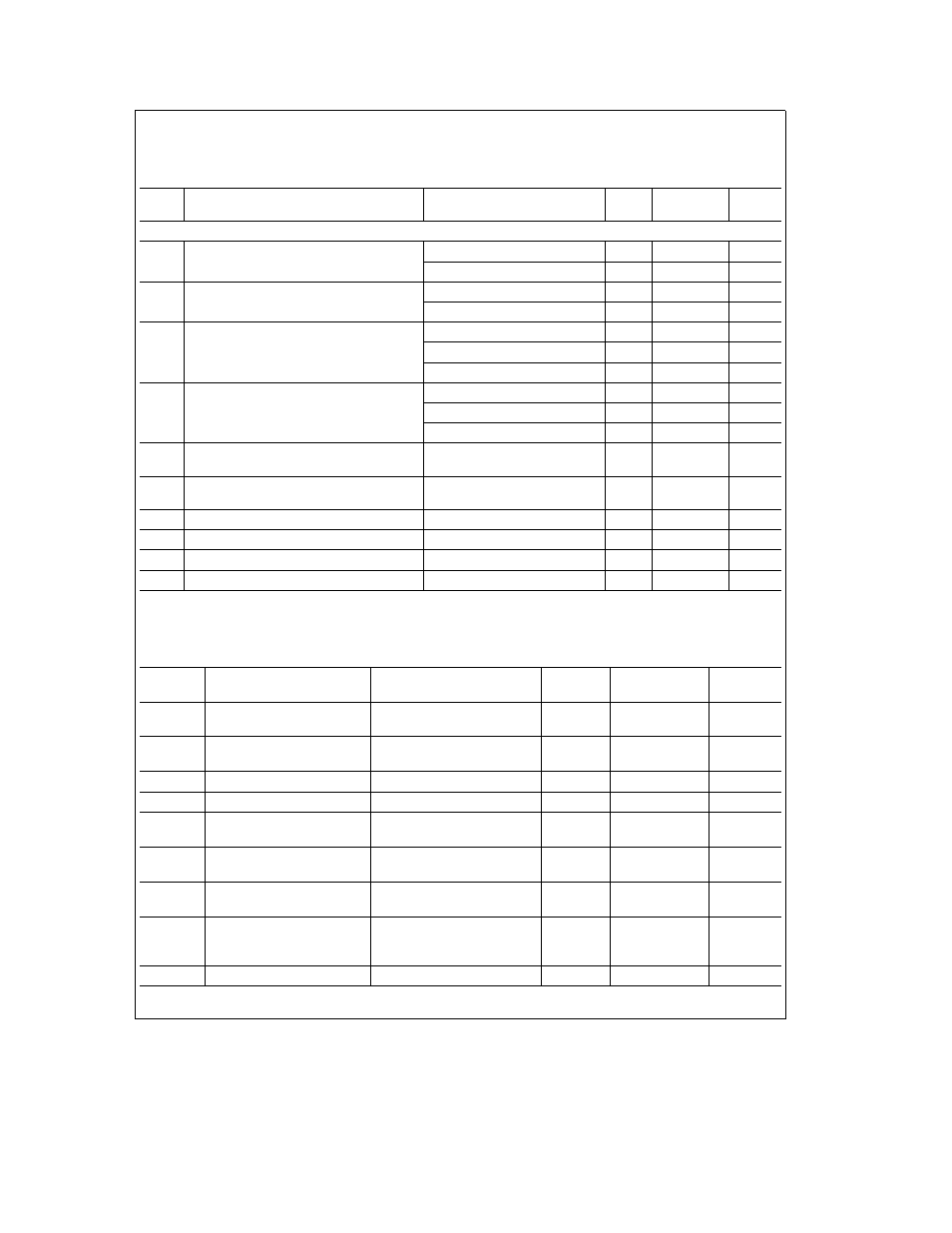
Converter Electrical Characteristics
The following specifications apply for V
CC
e
DV
CC
e
AV
CC
e a
5 0V V
b
e b
5 0V V
REF
e a
5 0V Analog Input Source
Impedance e 600X and f
CLK
e
2 0 MHz unless otherwise specified Boldface limits apply for T
A
e
T
J
e
T
MIN
to T
MAX
all other limits T
A
e
T
J
e
25 C (Notes 6 7 and 8) (Continued)
Symbol
Parameter
Conditions
Typical
Limit
Units
(Note 9) (Notes 10 19)
(Limit)
DYNAMIC CHARACTERISTICS
(Continued)
THD
Bipolar Total Harmonic Distortion
f
IN
e
1 kHz V
IN
e
g
4 85V
b
82
dB
(Note 17)
f
IN
e
19 688 kHz V
IN
e
g
4 85V
b
80
b
75
dB (max)
THD
Unipolar Total Harmonic Distortion
f
IN
e
1 kHz V
IN
e
4 85 V
p-p
b
82
dB
(Note 17)
f
IN
e
19 688 kHz V
IN
e
4 85 V
p-p
b
80
b
75
dB (max)
Bipolar Peak Harmonic or
f
IN
e
1 kHz V
IN
e
g
4 85V
b
88
dB
Spurious Noise (Note 17)
f
IN
e
10 kHz V
IN
e
g
4 85V
b
84
dB
f
IN
e
20 kHz V
IN
e
g
4 85V
b
80
dB
Unipolar Peak Harmonic or
f
IN
e
1 kHz V
IN
e
4 85 V
p-p
b
90
dB
Spurious Noise (Note 17)
f
IN
e
10 kHz V
IN
e
4 85 V
p-p
b
86
dB
f
IN
e
20 kHz V
IN
e
4 85 V
p-p
b
82
dB
Bipolar Two Tone Intermodulation
V
IN
e
g
4 85V f
IN1
e
19 375 kHz
b
78
b
74
dB (max)
Distortion (Note 17)
f
IN2
e
20 625 kHz
Unipolar Two Tone Intermodulation
V
IN
e
4 85 V
p-p
f
IN1
e
19 375 kHz
b
78
b
73
dB (max)
Distortion (Note 17)
f
IN2
e
20 625 kHz
b
3 dB Bipolar Full Power Bandwidth
V
IN
e
g
4 85V (Note 17)
25
20
kHz (Min)
b
3 dB Unipolar Full Power Bandwidth
V
IN
e
4 85 V
p-p
(Note 17)
30
20
kHz (Min)
Aperture Time
100
ns
Aperture Jitter
100
ps
rms
Digital and DC Electrical Characteristics
The following specifications apply for DV
CC
e
AV
CC
e a
5 0V V
b
e b
5 0V V
REF
e a
5 0V and f
CLK
e
2 0 MHz unless
otherwise specified Boldface limits apply for T
A
e
T
J
e
T
MIN
to T
MAX
all other limits T
A
e
T
J
e
25 C
(Notes 6 and 7)
Symbol
Parameter
Conditions
Typical
Limit
Units
(Note 9)
(Notes 10 19)
(Limits)
V
IN(1)
Logical ‘‘1’’ Input Voltage for
V
CC
e
5 25V
2 0
V (min)
All Inputs except CLK IN
V
IN(0)
Logical ‘‘0’’ Input Voltage for
V
CC
e
4 75V
0 8
V (max)
All Inputs except CLK IN
I
IN(1)
Logical ‘‘1’’ Input Current
V
IN
e
5V
0 005
1
m
A (max)
I
IN(0)
Logical ‘‘0’’ Input Current
V
IN
e
0V
b
0 005
b
1
m
A (max)
V
T
a
CLK IN Positive-Going
2 8
2 7
V (min)
Threshold Voltage
V
T
b
CLK IN Negative-Going
2 1
2 3
V (max)
Threshold Voltage
V
H
CLK IN Hysteresis
0 7
0 4
V (min)
V
T
a
(min) b V
T
b
(max)
V
OUT(1)
Logical ‘‘1’’ Output Voltage
V
CC
e
4 75V
I
OUT
e b
360 mA
2 4
V (min)
I
OUT
e b
10 mA
4 5
V (min)
V
OUT(0)
Logical ‘‘0’’ Output Voltage
V
CC
e
4 75V I
OUT
e
1 6 mA
0 4
V (max)
3