3 0 analog considerations – Rainbow Electronics ADC12441 User Manual
Page 12
3 0 Analog Considerations
(Continued)
For absolute accuracy where the analog input varies be-
tween very specific voltage limits the reference pin can be
biased with a time and temperature stable voltage source
In general the magnitude of the reference voltage will re-
quire an initial adjustment to null out full-scale errors
3 2 INPUT CURRENT
Because the input network of the ADC12441 is made up of
a switch and a network of capacitors a charging current will
flow into or out of (depending on the input voltage polarity)
of the analog input pin (V
IN
) on the start of the analog input
sampling period (t
A
) The peak value of this current will de-
pend on the actual input voltage applied
3 3 NOISE
The leads to the analog input pin should be kept as short as
possible to minimize input noise coupling Both noise and
undesired digital clock coupling to this input can cause er-
rors Input filtering can be used to reduce the effects of
these noise sources
3 4 INPUT BYPASS CAPACITORS
An external capacitor can be used to filter out any noise due
to inductive pickup by a long input lead and will not degrade
the accuracy of the conversion result
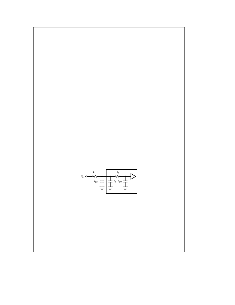
3 5 INPUT SOURCE RESISTANCE
The analog input can be modeled as shown in
Figure 3
External R
S
will lengthen the time period necessary for the
voltage on C
REF
to settle to within
LSB of the analog
input voltage With f
CLK
e
2 MHz t
A
e
7 clock periods e
3 5 ms R
S
s
1 kX will allow a 5V analog input voltage to
settle properly
3 6 POWER SUPPLIES
Noise spikes on the V
CC
and V
b
supply lines can cause
conversion errors as the comparator will respond to this
noise The A D is especially sensitive during the auto-zero
or auto-cal procedures to any power supply spikes Low in
ductance tantalum capacitors of 10 mF or greater paralleled
with 0 1 mF ceramic capacitors are recommended for supply
bypassing Separate bypass capacitors whould be placed
close to the DV
CC
AV
CC
and V
b
pins If an unregulated
voltage source is available in the system
a separate
LM340LAZ-5 0 voltage regulator for the A-to-D’s V
CC
(and
other analog circuitry) will greatly reduce digital noise on the
supply line
3 7 THE CALIBRATION CYCLE
On power up the ADC12441 goes through an Auto-Cal cy-
cle which cannot be interrupted Since the power supply
reference and clock will not be stable at power up this first
calibration cycle will not result in an accurate calibration of
the A D A new calibration cycle needs to be started after
the power supplies reference and clock have been given
enough time to stabilize During the calibration cycle cor-
rection values are determined for the offset voltage of the
sampled data comparator and any linearity and gain errors
These values are stored in internal RAM and used during an
analog-to-digital conversion to bring the overall full scale
offset and linearity errors down to the specified limits Full
scale error typically changes
g
0 1 LSB over temperature
and linearity error changes even less therefore it should be
necessary to go through the calibration cycle only once af-
ter power up if auto-zero is used to correct the zero error
change
3 8 THE AUTO-ZERO CYCLE
To correct for any change in the zero (offset) error of the
A D the auto-zero cycle can be used It may be necessary
to do an auto-zero cycle whenever the ambient temperature
changes significantly (See the curved titled ‘‘Zero Error
Change vs Ambient Temperature’’ in the Typical Perform-
ance Characteristics ) A change in the ambient temperature
will cause the V
OS
of the sampled data comparator to
change which may cause the zero error of the A D to be
greater than
g
1 LSB An auto-zero cycle will maintain the
zero error to
g
1 LSB or less
TL H 11017 – 21
FIGURE 3 Analog Input Equivalent Circuit
12