Rainbow Electronics MAX4912 User Manual
Page 9
MAX4910/MAX4911/MAX4912
Quad-SPDT, Clickless Audio Switches
with Negative Signal Handling
_______________________________________________________________________________________
9
Analog Signal Levels
The MAX4910/MAX4911/MAX4912 on-resistance is
channel dependant. Channels 1 and 3 have an on-
resistance of 0.37
Ω (typ), and channels 2 and 4 have
an on-resistance of 0.72
Ω (typ). The on-resistance flat-
ness is guaranteed over temperature and shows mini-
mal variation over the entire voltage supply range (see
the Typical Operating Characteristics). The on-resis-
tance flatness and low-leakage features make it ideal
for bidirectional operation. The switches are bidirection-
al, so the NO_, NC_, and COM_ pins can be either
inputs or outputs.
These devices pass signals as low as V
CC
- 5.5V,
including signals below ground with minimal distortion.
Click-and-Pop Suppression
The MAX4910/MAX4911 have a 3.8k
Ω (typ) shunt resis-
tor on all their NO and NC terminals to automatically
discharge any capacitance when they are not connect-
ed to COM. The MAX4912 has shunt resistors on all
NO, NC1, and NC3 terminals. The shunt resistors
reduce audible click-and-pop sounds that occur when
switching between audio sources.
Audible clicks and pops are caused when a step DC
voltage is switched into the speaker. The DC step tran-
sients can be reduced by automatically discharging the
side that is not connected to the COM terminal, reducing
any residual DC voltage and reducing clicks and pops.
Break-Before-Make Switching
The MAX4910/MAX4911/MAX4912 feature break-
before-make switching, which is configured to break
(open) the first set of contacts before engaging (clos-
ing) the new contacts. This prevents the momentary
connection of the old and new signal paths to the out-
put, reducing click-and-pop sounds.
Power-Supply Sequencing and
Overvoltage Protection
Caution: Do not exceed the Absolute Maximum
Ratings since stresses beyond the listed ratings
may cause permanent damage to the device.
Proper power-supply sequencing is recommended for
all CMOS devices. Improper supply sequencing can
force the switch into latchup causing it to draw exces-
sive supply current. The only way out of latchup is to
recycle the power and properly reapply it. Connect all
ground pins first, then apply power to V
CC
, and finally
apply signals to NO_, NC_, and COM_. Follow the
reverse order upon power-down.
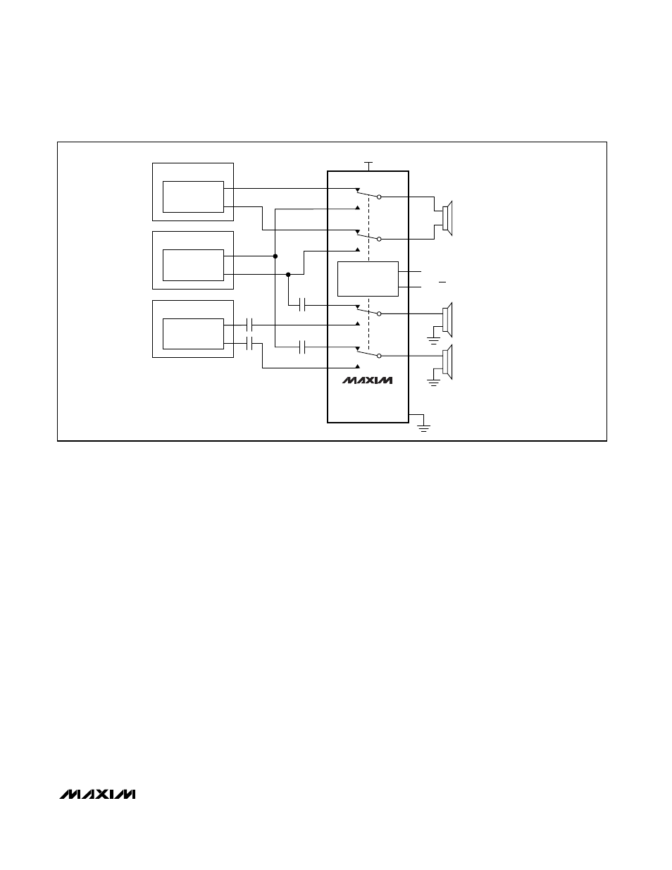
GND
V
CC
1.8V TO 5.5V
NO2
COM2
NC4
NO4
COM4
NC2
VOICE
AMP
MELODY IC
CODEC
CODEC
MP3
CB1 (CB)
DISCHARGE
CONTROL/
SIGNAL CONTROL
CB2 (EN)
NO1
COM1
NC3
NC1
NO3
COM3
SPEAKER 8
Ω
MAX4910
MAX4911
MAX4912
( ) IS FOR MAX4911 ONLY
Figure 1. Typical Application Circuit