Electrical characteristics (continued) – Rainbow Electronics MAX4912 User Manual
Page 3

MAX4910/MAX4911/MAX4912
Quad-SPDT, Clickless Audio Switches
with Negative Signal Handling
_______________________________________________________________________________________
3
Note 1: All parameters are production tested at T
A
= +85°C and guaranteed by design over the specified temperature range.
Note 2: Signals on COM_, NO_, or NC_ exceeding V
CC
are clamped by internal diodes. Limit forward-diode current to maximum current
rating.
Note 3: Guaranteed by design; not production tested.
Note 4:
∆R
ON
= R
ON(MAX)
- R
ON(MIN)
.
Note 5: Flatness is defined as the difference between the maximum and minimum value of on-resistance as measured over the specified
analog signal ranges.
Note 6: Off-isolation = 20log
10
[V
COM_
/ V
NO_
], V
COM_
= output, V
NO
_ = input to off switch.
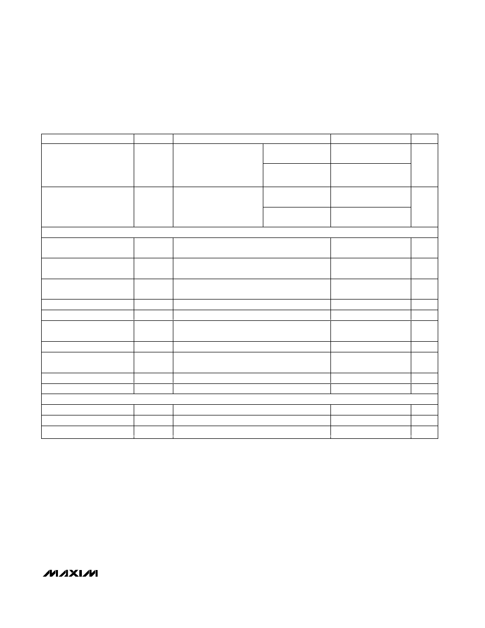
ELECTRICAL CHARACTERISTICS (continued)
(V
CC
= +2.7V to +5.5V, T
A
= -40°C to +85°C, EN = low (MAX4911 only), unless otherwise noted. Typical values are at V
CC
= +3.0V, T
A
=
+25°C.) (Note 1)
PARAMETER
SYMBOL
CONDITIONS
MIN
TYP
MAX
UNITS
T
A
= +25°C
-10
+10
NC_ Off-Leakage Current
I
NC_(OFF)
MAX4912 (NC2 and NC4)
only: V
CC
= +2.7V, switch
open, V
NC_
= -2.5V or
+2.5V, V
COM_
= +2.5V or
-2.5V
T
A
= T
MIN
to T
MAX
-50
+50
nA
T
A
= +25°C
-10
+10
COM_ On-Leakage Current
I
COM_(ON)
V
CC
= +2.7V, switch closed;
V
NC_
or V
NO_
= -2.5V,
+2.5V, or floating; V
COM_
=
-2.5V, +2.5V, or floating
T
A
= T
MIN
to T
MAX
-100
+100
nA
DYNAMIC CHARACTERISTICS
Turn-On Time
t
ON
V
CC
= +2.7V, CB_ = low to high, R
L
= 50
Ω,
C
L
= 5pF, V
NO_
= +1.5V, Figure 2
0.055
0.15
µs
Turn-Off Time
t
OFF
V
CC
= +2.7V, CB_ = high to low, R
L
= 50
Ω,
C
L
= 5pF, V
NO_
= +1.5V, Figure 2
0.3
1.0
µs
Break-Before-Make Delay
Time
t
D
V
C C
= + 2.7V , C B_ = l ow to hi g h or hi g h to l ow ,
R
L
= 50
Ω , C
L
= 5p F, V
N C _
= V
N O_
= + 1.5V , Fi g ur e 3
1
25
ns
Charge Injection
Q
V
GEN_
= 0, R
GEN
= 0, C
L
= 1nF, Figure 4
300
pC
P ow er - S up p l y Rej ecti on Rati o
PSRR
f = 20kHz, V
COM_
= 1V
RMS,
R
L
= 50
Ω, C
L
= 5pF
60
dB
Off-Isolation
V
ISO
f = 20kHz, V
COM_
= 1V
RMS
, R
L
= 50
Ω, Figure 5
(Note 6)
-90
dB
Crosstalk
V
CT
f = 20kHz, V
COM_
= 1V
RMS
, R
L
= 50
Ω, Figure 5
-80
dB
Total Harmonic Distortion
THD
f = 20Hz to 20kHz, V
COM_
= 0.5V
P-P
, R
L
= 50
Ω,
DC bias = 0
0.05
%
NO_, NC_
Off-Capacitance
C
NO
_
(OFF)
f = 1M H z, V
C OM _
= 0.5V
P - P
,
D C b i as = 0, Fi g ur e 6
100
pF
COM
On-Capacitance
C
COM
_
(ON)
f = 1M H z, V
C OM _
= 0.5V
P - P
, D C b i as = 0, Fi g ur e 6
200
pF
DIGITAL INPUTS (CB_,
EN)
Input Logic High
V
IH
1.4
V
Input Logic Low
V
IL
0.5
V
Input Leakage Current
I
CB
,
I
EN
V
CB
_ = V
EN
= 0V or V
CC
-1
+1
µA
