Rainbow Electronics ADC12038 User Manual
General description, Applications, Features
TL H 11354
ADC12H030ADC12H032ADC12H034ADC12H038
ADC12030ADC12032ADC12034ADC12038
Self-Calibrating
12-Bit
Plus
Sign
Serial
IO
AD
Converters
with
MUX
and
SampleHold
January 1995
ADC12H030 ADC12H032 ADC12H034 ADC12H038
ADC12030 ADC12032 ADC12034 ADC12038
Self-Calibrating 12-Bit Plus Sign Serial I O
A D Converters with MUX and Sample Hold
General Description
The ADC12030 and ADC12H030 families are 12-bit plus
sign successive approximation A D converters with serial
I O and configurable input multiplexers The ADC12032
ADC12H032
ADC12034 ADC12H034 and ADC12038
ADC12H038 have 2 4 and 8 channel multiplexers respec-
tively The differential multiplexer outputs and A D inputs
are available on the MUXOUT1 MUXOUT2 A DIN1 and
A DIN2 pins The ADC12030 ADC12H030 has a two chan-
nel multiplexer with the multiplexer outputs and A D inputs
internally connected The ADC12030 family is tested with a
5 MHz clock while the ADC12H030 family is tested with an
8 MHz clock On request these A Ds go through a self
calibration process that adjusts linearity zero and full-scale
errors to less than
g
1 LSB each
The analog inputs can be configured to operate in various
combinations of single-ended differential or pseudo-differ-
ential modes A fully differential unipolar analog input range
(0V to a5V) can be accommodated with a single a5V sup-
ply In the differential modes valid outputs are obtained
even when the negative inputs are greater than the positive
because of the 12-bit plus sign output data format
The serial I O is configured to comply with the NSC
MICROWIRE
TM
For complementary voltage references see
the LM4040 LM4041 or LM9140
Applications
Y
Medical instruments
Y
Process control systems
Y
Test equipment
Features
Y
Serial I O (MICROWIRE Compatible)
Y
2 4 or 8 channel differential or single-ended
multiplexer
Y
Analog input sample hold function
Y
Power down mode
Y
Variable resolution and conversion rate
Y
Programmable acquisition time
Y
Variable digital output word length and format
Y
No zero or full scale adjustment required
Y
Fully tested and guaranteed with a 4 096V reference
Y
0V to 5V analog input range with single 5V power
supply
Y
No Missing Codes over temperature
Key Specifications
Y
Resolution
12-bit plus sign
Y
12-bit plus sign conversion time
ADC12H030 family
5 5 ms (max)
ADC12030 family
8 8 ms (max)
Y
12-bit plus sign throughput time
ADC12H030 family
8 6 ms (max)
ADC12030 family
14 ms (max)
Y
Integral linearity error
g
1 LSB (max)
Y
Single supply
5V
g
10%
Y
Power dissipation
33 mW (max)
Power down
100 mW (typ)
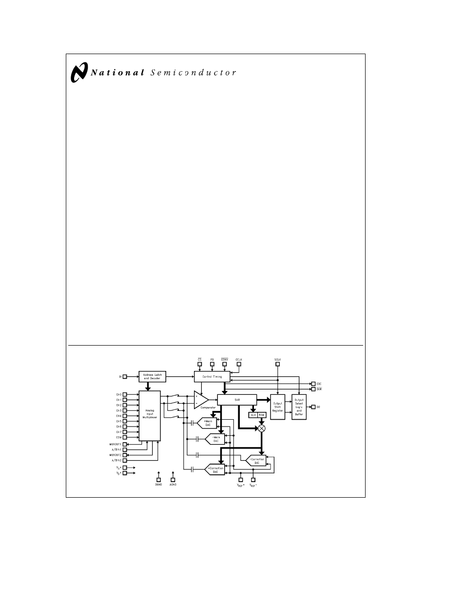
ADC12038 Simplified Block Diagram
TL H 11354 – 1
TRI-STATE
is a registered trademark of National Semiconductor Corporation
COPS
TM
microcontrollers HPC
TM
and MICROWIRE
TM
are trademarks of National Semiconductor Corporation
C1995 National Semiconductor Corporation
RRD-B30M75 Printed in U S A