Rainbow Electronics MAX9717 User Manual
Page 11
Adjustable Gain
Gain-Setting Resistors
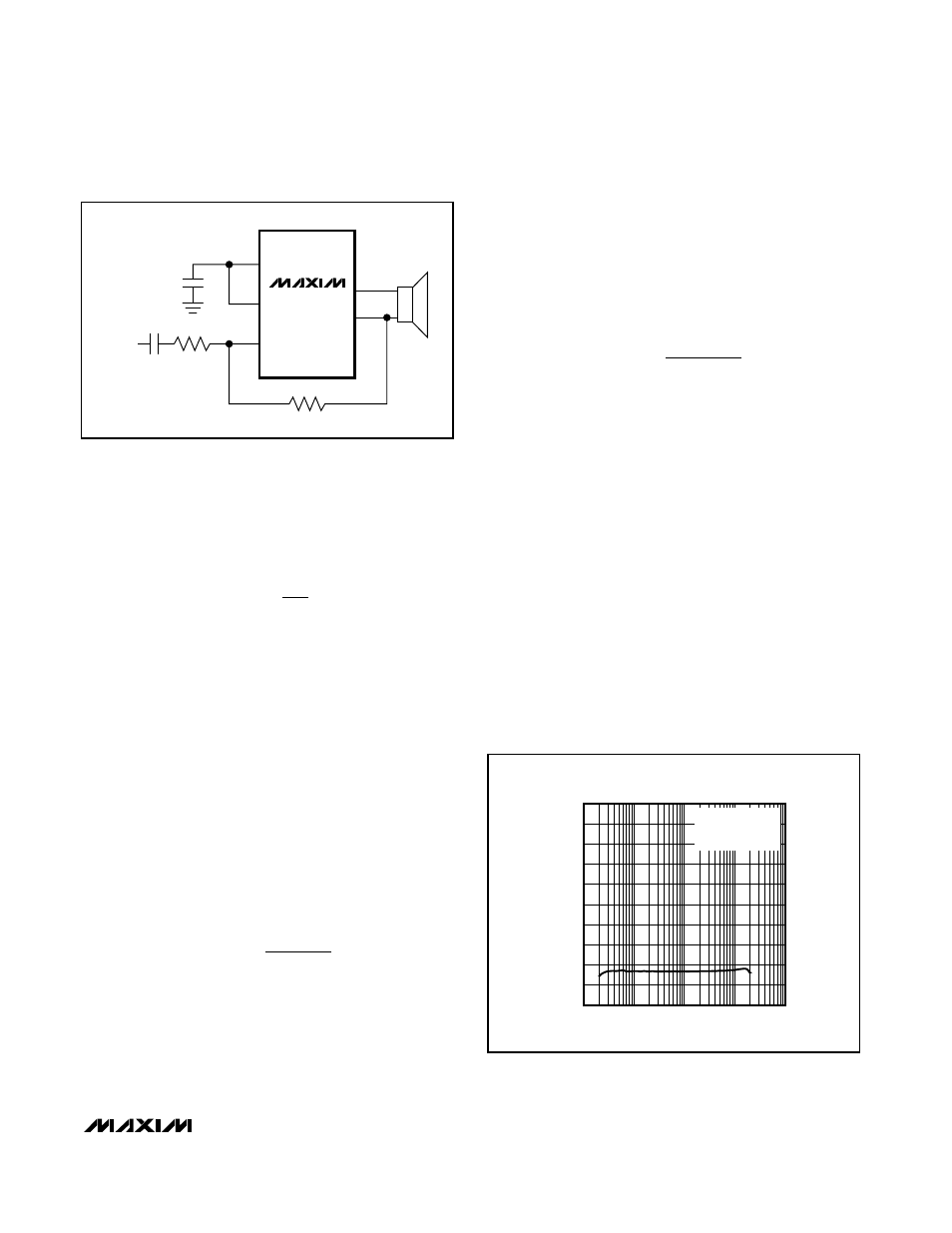
External feedback resistors set the gain of the
MAX9716 and MAX9717A. Resistors R
F
and R
IN
(see
Figure 2) set the gain of the amplifier as follows:
Where A
V
is the desired voltage gain. Hence, an R
IN
of
20k
Ω and an R
F
of 20k
Ω yields a gain of 2V/V, or 6dB.
R
F
can be either fixed or variable, allowing the use of a
digitally controlled potentiometer to alter the gain under
software control.
The gain of the MAX9717 in a single-ended output
configuration is half the gain when configured as BTL
output. Choose R
F
between 10k
Ω and 50kΩ for the
MAX9716 and MAX9717A. Gains for the MAX9717B/C/D
are set internally.
Input Filter
C
IN
and R
IN
form a highpass filter that removes the DC
bias from an incoming signal. The AC-coupling capaci-
tor allows the amplifier to bias the signal to an optimal
DC level. Assuming zero-source impedance, the -3dB
point of the highpass filter is:
Setting f
-3dB
too high affects the low-frequency
response of the amplifier. Use capacitors with
dielectrics that have low-voltage coefficients, such as
tantalum or aluminum electrolytic. Capacitors with high-
voltage coefficients, such as ceramics, can increase
distortion at low frequencies.
Output-Coupling Capacitor
The MAX9717 require output-coupling capacitors to
operate in single-ended (headphone) mode. The out-
put-coupling capacitor blocks the DC component of the
amplifier output, preventing DC current from flowing to
the load. The output capacitor and the load impedance
form a highpass filter with a -3dB point determined by:
As with the input capacitor, choose C
OUT
such that
f
-3dB
is well below the lowest frequency of interest.
Setting f
-3dB
too high affects the amplifier’s low-fre-
quency response. Load impedance is a concern when
choosing C
OUT
. Load impedance can vary, changing
the -3dB point of the output filter. A lower impedance
increases the corner frequency, degrading low-fre-
quency response. Select C
OUT
such that the worst-
case load/C
OUT
combination yields an adequate
response. Select capacitors with low ESR to minimize
resistive losses and optimize power transfer to the load.
Differential Input
The MAX9716 can be configured for a differential input.
The advantage of differential inputs is that any com-
mon-mode noise is attenuated and not passed through
the amplifier. This input improves noise rejection and
provides common-mode rejection (Figure 3). External
components should be closely matched for high
CMRR. Figure 4 shows the MAX9716 configured for a
differential input.
f
R C
dB
L OUT
−
=
3
1
2
π
f
R C
dB
IN IN
−
=
3
1
2
π
A
R
R
V
F
IN
=
⎛
⎝⎜
⎞
⎠⎟
2
MAX9716/MAX9717
Low-Cost, Mono, 1.4W BTL Audio Power
Amplifiers
______________________________________________________________________________________
11
OUT-
OUT+
MAX9716
R
F
IN-
IN+
BIAS
R
IN
C
IN
AUDIO
INPUT
Figure 2. Setting the MAX9716/MAX9717A Gain
FREQUENCY (Hz)
CMRR (dB)
10k
1k
100
-90
-80
-70
-60
-50
-40
-30
-20
-10
0
-100
10
100k
V
RIPPLE
= 200mV
P-P
R
L
= 8
Ω
C
BIAS
= 1
µF
COMMON-MODE REJECTION RATIO
vs. FREQUENCY
Figure 3. CMRR with Differential Input