Rainbow Electronics MAX9589 User Manual
Page 2
MAX9586–MAX9589
Single, Dual, Triple, and Quad Standard-Definition
Video Filter Amplifiers with AC-Coupled Input Buffers
2
_______________________________________________________________________________________
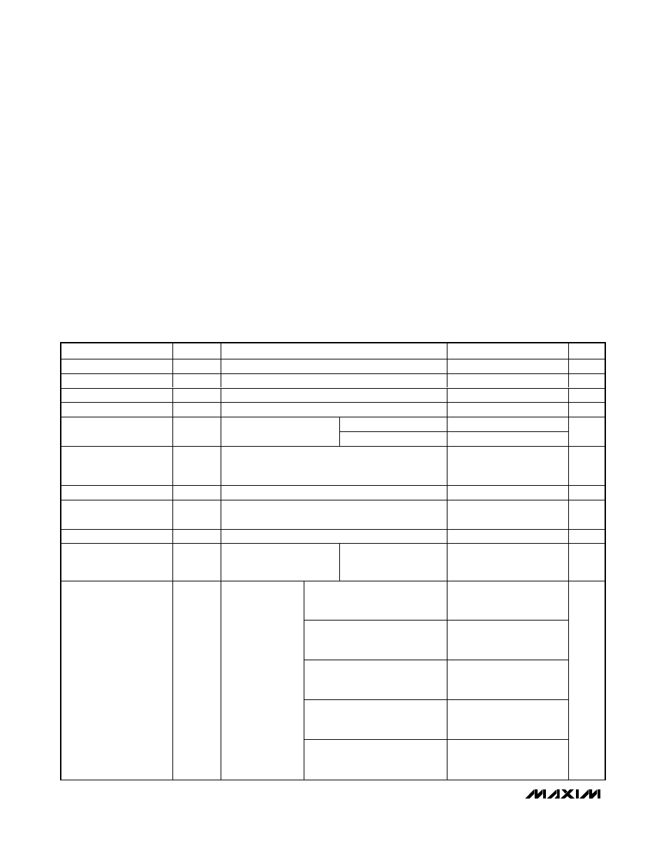
ABSOLUTE MAXIMUM RATINGS
ELECTRICAL CHARACTERISTICS
(V
DD
= 3.3V, GND = 0V, VR
L
= no load, T
A
= T
MIN
to T
MAX
, unless otherwise noted. Typical values are at T
A
= +25°C.) (Note 1)
Stresses beyond those listed under “Absolute Maximum Ratings” may cause permanent damage to the device. These are stress ratings only, and functional
operation of the device at these or any other conditions beyond those indicated in the operational sections of the specifications is not implied. Exposure to
absolute maximum rating conditions for extended periods may affect device reliability.
V
DD
to GND ..............................................................-0.3V to +4V
IN_ to GND ...............................................................-0.3V to +4V
SHDN to GND...........................................................-0.3V to +4V
OUT_ Short Circuit Duration to V
DD
, GND .................Continuous
Continuous Input Current
IN_, SHDN ....................................................................±20mA
Continuous Power Dissipation (T
A
= +70°C)
5-Pin Thin SOT23 (derate 9.1mW/°C above +70°C) ....727mW
6-Pin TDFN (derate 18.2mW/°C above +70°C) .........1455mW
6-Pin Thin SOT23 (derate 9.1mW/°C above +70°C) ....727mW
6-Pin µDFN (derate 4.5mW/°C above +70°C) .............358mW
8-Pin µDFN (derate 4.8mW/°C above +70°C) ..........380.6mW
8-Pin µMAX (derate 4.5mW/°C above +70°C) .............362mW
10-Pin µMAX (derate 5.6mW/°C above +70°C) ...........444mW
12-Pin 3mm x 3mm TQFN (derate 14.7mW/°C
above +70°C).............................................................1177mW
Operating Temperature Range .........................-40°C to +125°C
Junction Temperature ......................................................+150°C
Storage Temperature Range .............................-65°C to +150°C
Lead Temperature (soldering, 10s) .................................+300°C
PARAMETER
SYMBOL
CONDITIONS
MIN
TYP
MAX
UNITS
Supply Voltage Range
V
DD
Guaranteed by PSRR
2.7
3.6
V
Supply Current
I
DD
Per channel
4.25
8
mA
Shutdown Supply Current
I
SHDN
SHDN = GND
0.01
1
µA
Sync-Tip Clamp Level
V
CLP
Sync-tip clamp
0.23
0.39
V
V
DD
= 2.7V to 3.6V
1.05
Input Voltage Range
V
IN
Guaranteed by output
voltage swing
V
DD
= 3V to 3.6V
1.2
V
P-P
Sync Crush
Sync-tip clamp, percentage reduction in sync pulse
(0.3V
P-P
), guaranteed by input clamping current
measurement, measured at input
2
%
Input Clamping Current
Sync-tip clamp
1
2
µA
Maximum Input Source
Resistance
300
Ω
DC Voltage Gain (Note 2)
A
V
Guaranteed by output voltage swing
1.95
2
2.04
V/V
Output Level
Measured at V
OUT
,
IN_ = 0.1µF to GND,
R
L
= 150Ω to GND
Sync-tip clamp
0.22
0.3
0.39
V
Measured at output, V
DD
= 2.7V,
V
IN
= V
CLP
to (V
CLP
+ 1.05V),
R
L
= 150Ω to -0.2V
2.058
2.1
2.142
Measured at output, V
DD
= 2.7V,
V
IN
= V
CLP
to (V
CLP
+ 1.05V),
R
L
= 150Ω to V
DD
/2
2.058
2.1
2.142
Measured at output, V
DD
= 3V,
V
IN
= V
CLP
to (V
CLP
+ 1.2V),
R
L
= 150Ω to -0.2V
2.340
2.4
2.448
Measured at output, V
DD
= 3V,
V
IN
= V
CLP
to (V
CLP
+ 1.2V),
R
L
= 150Ω to V
DD
/2
2.340
2.4
2.448
Output-Voltage Swing
Sync-tip clamp
Measured at output, V
DD
=
3.135V, V
IN
= V
CLP
to (V
CLP
+
1.05V), R
L
= 75Ω to -0.2V
2.027
2.1
2.163
V
P-P