Smbus digital interface, Temperature reading – Rainbow Electronics MAX6640 User Manual
Page 7
SMBus Digital Interface
From a software perspective, the MAX6640 appears as
a set of byte-wide registers. This device uses a stan-
dard SMBus 2-wire/I
2
C™-compatible serial interface to
access the internal registers.
The MAX6640 employs four standard SMBus protocols:
write byte, read byte, send byte, and receive byte
(Figures 1, 2, and 3). The shorter receive byte protocol
allows quicker transfers, provided that the correct data
register was previously selected by a read byte instruc-
tion. Use caution with the shorter protocols in multimas-
ter systems, since a second master could overwrite the
command byte without informing the first master.
Table 3 details the register addresses and functions,
whether they can be read or written to, and the power-
on reset (POR) state. See Tables 4–8 for all other regis-
ter functions and the Register Descriptions section.
Temperature Reading
Temperature data can be read from registers 00h and
01h. The temperature data format for these registers is
8 bits, with the LSB representing 1°C (Table 1) and the
MSB representing +128°C. The MSB is transmitted first.
Three additional temperature bits provide resolution
down to 0.125°C and are in the channel 1 extended
temperature (05h) and channel 2 extended tempera-
ture (06h) registers. All values below 0°C clip to 00h.
The MAX6640 employs a register lock mechanism to
avoid getting temperature results from the temperature
register and the extended temperature register sam-
pled at two different time points. Reading the extended
register stops the MAX6640 from updating the temper-
ature register for at least 0.25s, unless there is a tem-
MAX6640
2-Channel Temperature Monitor with Dual
Automatic PWM Fan-Speed Controller
_______________________________________________________________________________________
7
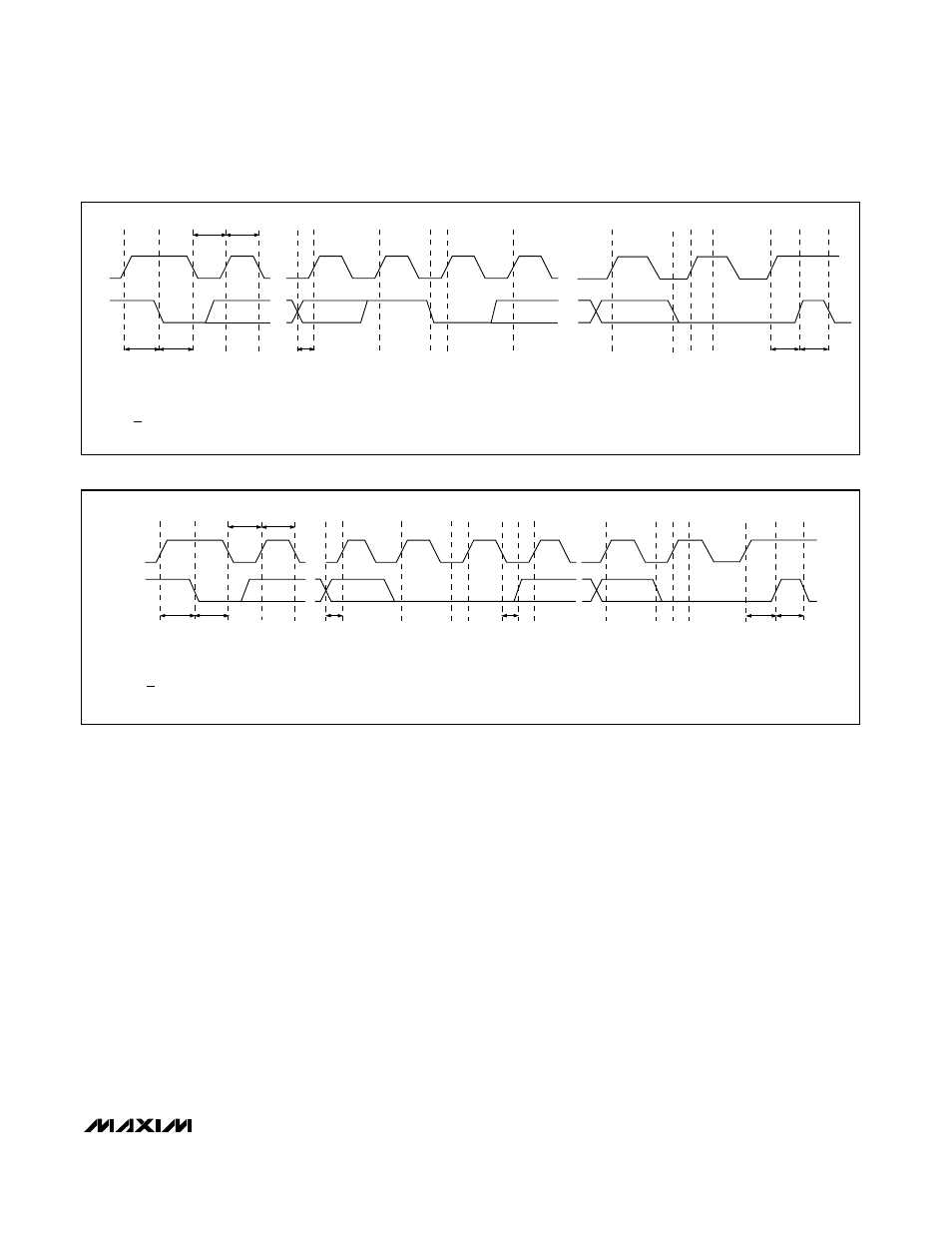
SCL
A = START CONDITION
B = MSB OF ADDRESS CLOCKED INTO SLAVE
C = LSB OF ADDRESS CLOCKED INTO SLAVE
D = R/W BIT CLOCKED INTO SLAVE
A
B
C
D
E
F
G
H
I
J
SDA
t
SU:STA
t
HD:STA
t
LOW
t
HIGH
t
SU:DAT
t
SU:STO
t
BUF
L
M
K
E = SLAVE PULLS SMBDATA LINE LOW
F = ACKNOWLEDGE BIT CLOCKED INTO MASTER
G = MSB OF DATA CLOCKED INTO SLAVE
H = LSB OF DATA CLOCKED INTO SLAVE
I = MASTER PULLS DATA LINE LOW
J = ACKNOWLEDGE CLOCKED INTO SLAVE
K = ACKNOWLEDGE CLOCK PULSE
L = STOP CONDITION
M = NEW START CONDITION
Figure 2. SMBus Write Timing Diagram
SCL
A
B
C
D
E
F
G
H
I
J
K
SDA
t
SU:STA
t
HD:STA
t
LOW
t
HIGH
t
SU:DAT
t
HD:DAT
t
SU:STO
t
BUF
A = START CONDITION
B = MSB OF ADDRESS CLOCKED INTO SLAVE
C = LSB OF ADDRESS CLOCKED INTO SLAVE
D = R/W BIT CLOCKED INTO SLAVE
E = SLAVE PULLS SMBDATA LINE LOW
L
M
F = ACKNOWLEDGE BIT CLOCKED INTO MASTER
G = MSB OF DATA CLOCKED INTO MASTER
H = LSB OF DATA CLOCKED INTO MASTER
I = MASTER PULLS DATA LINE LOW
J = ACKNOWLEDGE CLOCKED INTO SLAVE
K = ACKNOWLEDGE CLOCK PULSE
L = STOP CONDITION
M = NEW START CONDITION
Figure 3. SMBus Read Timing Diagram
I
2
C is a trademark of Philips Corp.
Purchase of I
2
C components of Maxim Integrated Products, Inc.,
or one of its sublicensed Associated Companies, conveys a
license under the Philips I
2
C Patent Rights to use these compo-
nents in an I
2
C system, provided that the system conforms to the
I
2
C Standard Specification as defined by Philips.