Chip information, Power consumption, Power-supply bypassing and ground – Rainbow Electronics MAX9656 User Manual
Page 12

MAX9655/MAX9656
Low-Power Video Switches
for Dual SCART Connectors
12
______________________________________________________________________________________
Power Consumption
The quiescent power consumption and average power
consumption of the MAX9655/MAX9656 are very low
because of the 3.3V operation and low-power circuit
design. Quiescent power consumption is defined when
the MAX9655/MAX9656 are operating without loads
and without any video signals.
Average power consumption represents the normal
power consumption when the devices drive real video
signals into real video loads. It is measured when the
MAX9655/MAX9656 drive a 150
Ω load to ground with
a 50% flat field, which serves as a proxy for a real
video signal.
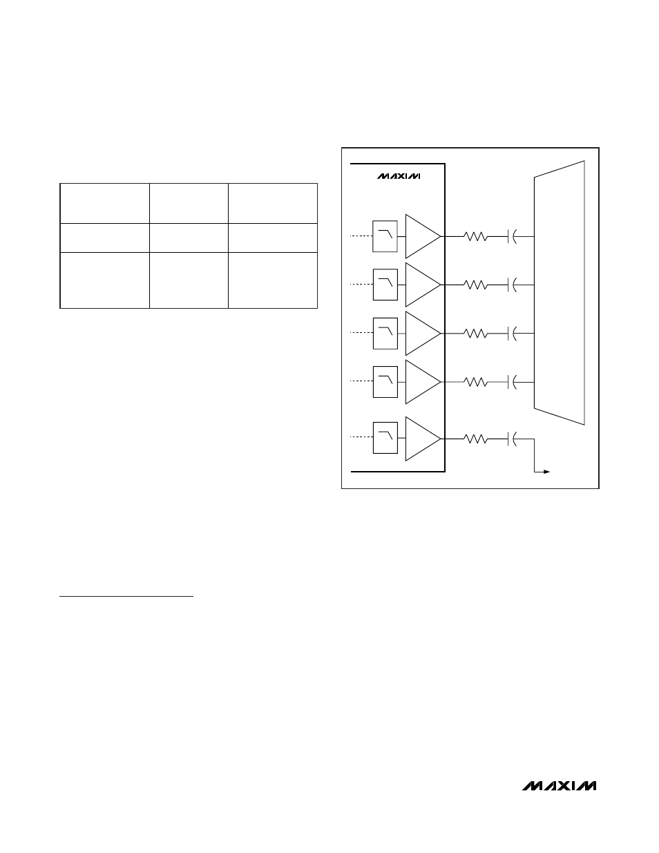
Table 6 shows the quiescent and average power con-
sumption of the MAX9655/MAX9656.
Power-Supply Bypassing and Ground
The MAX9655/MAX9656 operate from a single-supply
voltage down to 2.7V, allowing for low-power operation.
Bypass V
DD
to GND with a 0.1µF capacitor. Place
all external components as close as possible to
the device.
Chip Information
PROCESS: BiCMOS
A
V
= 2V/V
A
V
= 2V/V
A
V
= 2V/V
A
V
= 2V/V
A
V
= 2V/V
TV_B_OUT
TV_G_OUT
TV_R_OUT
TV_CVBS_OUT
TV SCART
220
μF
220
μF
220
μF
220
μF
220
μF
75
Ω
VCR_CVBS_OUT
LPF
LPF
LPF
LPF
LPF
TO VCR SCART
MAX9655
MAX9656
75
Ω
75
Ω
75
Ω
75
Ω
Figure 3. AC-Coupled Outputs
MEASUREMENTS
POWER
CONSUMPTION
(mW)
CONDITIONS
Quiescent Power
Consumption
69
No load.
Average Power
Consumption
175
150
Ω to ground on
each output. 50%
flat field signal on
each input.
Table 6. Quiescent and Average Power
Consumption for MAX9655/MAX9656
