2 0 functional description, 3 0 applications information – Rainbow Electronics ADC10158 User Manual
Page 18
2 0 Functional Description
(Continued)
Digital Interface Hints
Reads and writes can be completely asynchronous to
CLK
In addition to the timing indicated in Diagrams 1 – 3 CS
can be tied low permanently or taken low for entire con-
versions eliminating all the CS guardbands (t
CR
t
RC
t
CW
t
WC
)
If CS is used as shown in Diagrams 1–3 the CS guard-
bands (t
CR
t
RC
t
CW
t
WC
) between CS and the RD and
WR signals can safely be ignored as long as the following
two conditions are met
1) When initiating a write CS and WR must be simulta-
neously low for at least t
W(WR)
ns (see Diagram 1)
The ‘‘start’’ conversion’’ bit will be set on the rising
edge of WR or CS whichever is first
2) When reading data understand that data will not be
valid until t
ACC
ns after
both
CS and RD go low The
output data will enter TRI-STATE t
1H
ns or t
0H
ns after
either
CS or RD goes high (see Diagrams 2 and 3)
2 2 ARCHITECTURE
Before a conversion is started during the analog input sam-
pling period the sampled data comparator is zeroed As the
comparator is being zeroed the channel assigned to be the
positive input is connected to the A D’s input capacitor
(See the Digital Interface section for a description of the
assignment procedure ) This charges the input 32C capaci-
tor of the DAC to the positive analog input voltage The
switches shown in the DAC portion of the detailed block
diagram are set for this zeroing acquisition period The volt-
age at the input and output of the comparator are at equilib-
rium at this point in time When the conversion is started the
comparator feedback switches are opened and the 32C in-
put capacitor is then switched to the assigned negative in-
put voltage When the comparator feedback switch opens a
fixed amount of charge is trapped on the common plates of
the capacitors The voltage at the input of the comparator
moves away from equilibrium when the 32C capacitor is
switched to the assigned negative input voltage causing the
output of the comparator to go high (‘‘1’’) or low (‘‘0’’) The
SAR next goes through an algorithm controlled by the out-
put state of the comparator that redistributes the charge on
the capacitor array by switching the voltage on one side of
the capacitors in the array The objective of the SAR algo-
rithm is to return the voltage at the input of the comparator
as close as possible to equilibrium
The switch position information at the completion of the
successive approximation routine is a direct representation
of the digital output This information is then manipulated by
the Digital Output decoder to the programmed format The
reformatted data is then available to be strobed onto the
data bus (DB0 – DB7) via the digital output buffers by taking
CS and RD low
3 0 Applications Information
3 1 MULTIPLEXER CONFIGURATION
The design of these converters utilizes a sampled-data
comparator structure which allows a differential analog input
to be converted by the successive approximation routine
The actual voltage converted is always the difference be-
tween an assigned ‘‘a’’ input terminal and a ‘‘b’’ input ter-
minal The polarity of each input terminal or pair of input
terminals being converted indicates which line the converter
expects to be the most positive If the assigned ‘‘a’’ input is
less than the ‘‘b’’ input the converter responds with an all
zeros output code when configured for unsigned operation
When configured for signed operation the A D responds
with the appropriate output digital code
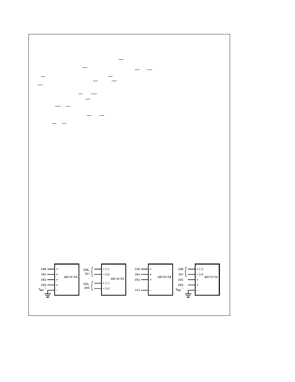
A unique input multiplexing scheme has been utilized to pro-
vide multiple analog channels The input channels can be
software configured into three modes differential single-
ended or pseudo-differential
Figure 3
shows the three
modes using the 4-channel MUX of the ADC10154 The
eight inputs of the ADC10158 can also be configured in any
of the three modes The single-ended mode has CH0 – CH3
assigned as the positive input with the negative input being
the V
REF
b
of the device In the differential mode the
ADC10154 channel inputs are grouped in pairs CH0 with
CH1 and CH2 with CH3 The polarity assignment of each
channel in the pair is interchangeable Finally in the pseu-
do-differential mode CH0 – CH2 are positive inputs referred
to CH3 which is now a pseudo-ground This pseudo-ground
input can be set to any potential within the input common-
mode range of the converter The analog signal conditioning
required in transducer-based data acquisition systems is
significantly simplified with this type of input flexibility One
converter package can now handle ground-referred inputs
and true differential inputs as well as signals referred to a
specific voltage
The analog input voltages for each channel can range from
50 mV below V
b
(typically ground for unipolar operation or
b
5V for bipolar operation) to 50 mV above V
a
e
DV
a
e
AV
a
(typically 5V) without degrading conversion accuracy
If the voltage on an unselected channel exceeds these lim-
its it may corrupt the reading of the selected channel
4 Single-Ended
2 Differential
3 Pseudo-Differential
2 Single Ended
and 1 Differential
TL H 11225 – 20
FIGURE 3 Analog Input Multiplexer Options
18