Timing diagrams – Rainbow Electronics ADC10158 User Manual
Page 13
Timing Diagrams
(Continued)
TL H 11225 – 17
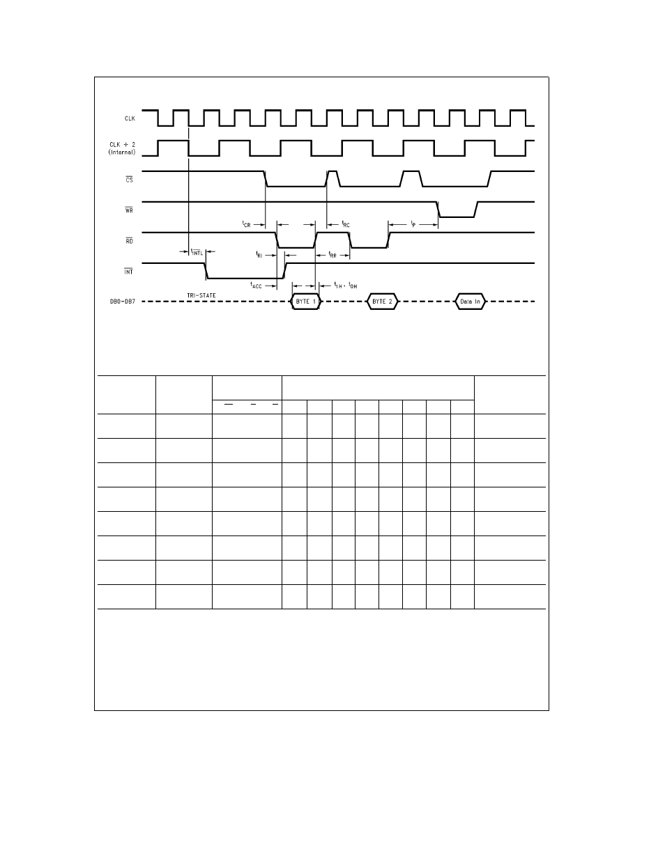
DIAGRAM 3 Reading the Conversion Result
Multiplexer Addressing and Output Data Configuration Tables
TABLE I ADC10154 and ADC10158 Output Data Configuration
Data Format
Output
Control Input
Data Bus Output Assignment
Resolution
Data
8 10
U S
L R
DB7
DB6
DB5
DB4
DB3
DB2
DB1
DB0
10-Bits a Sign
Right-Justified
L
L
L
Sign
Sign
Sign
Sign
Sign
Sign
MSB
9
First Byte Read
8
7
6
5
4
3
2
LSB
Second Byte Read
10-Bits a Sign
Left-Justified
L
L
H
Sign
MSB
9
8
7
6
5
4
First Byte Read
3
2
LSB
L
L
L
L
L
Second Byte Read
10-Bits
Right-Justified
L
H
L
L
L
L
L
L
L
MSB
9
First Byte Read
8
7
6
5
4
3
2
LSB
Second Byte Read
10-Bits
Left-Justified
L
H
H
MSB
9
8
7
6
5
4
3
First Byte Read
2
LSB
L
L
L
L
L
L
Second Byte Read
8-Bits a Sign
Right-Justified
H
L
L
Sign
Sign
Sign
Sign
Sign
Sign
Sign
Sign
First Byte Read
MSB
7
6
5
4
3
2
LSB
Second Byte Read
8-Bits a Sign
Left-Justified
H
L
H
Sign
MSB
7
6
5
4
3
2
First Byte Read
LSB
L
L
L
L
L
L
L
Second Byte Read
8-Bits
Right-Justified
H
H
L
L
L
L
L
L
L
L
L
First Byte Read
MSB
7
6
5
4
3
2
LSB
Second Byte Read
8-Bits
Left-Justified
H
H
H
MSB
7
6
5
4
3
2
LSB
First Byte Read
L
L
L
L
L
L
L
L
Second Byte Read
13