Thermal resistance characteristics, t, 25°c unless otherwise specified, Mechanical characteristics – C&H Technology CM100MXA-24S User Manual
Page 7: Recommended operating conditons, t, 25°c
CM100MXA-24S
NX-S Series CIB Module
(3Ø Converter + 3Ø Inverter + Brake)
100 Amperes/1200 Volts
Powerex, Inc., 173 Pavilion Lane, Youngwood, Pennsylvania 15697 (724) 925-7272 www.pwrx.com
6
05/11 Rev. 2
Thermal Resistance Characteristics,
T
j
= 25°C unless otherwise specified
Thermal Resistance, Junction to Case
*2
R
th(j-c)
Q
Per Inverter IGBT, per 1/6 Module
—
—
0.20
K/W
Thermal Resistance, Junction to Case
*2
R
th(j-c)
D
Per Inverter FWDi, per 1/6 Module
—
—
0.29
K/W
Thermal Resistance, Junction to Case
*2
R
th(j-c)
Q
Brake Part IGBT
—
—
0.35
K/W
Thermal Resistance, Junction to Case
*2
R
th(j-c)
D
Brake Part ClampDi
—
—
0.63
K/W
Thermal Resistance, Junction to Case
*2
R
th(j-c)
D
Converter Part ConvDi, per 1/6 Module
—
—
0.24
K/W
Contact Thermal Resistance,
R
th(c-s)
Thermal Grease Applied,
—
0.015
— K/W
Case to Heatsink
*2
per 1 Module
*7
Mechanical Characteristics
Mounting Torque M
s
Mounting to Heatsink, M5 Screw
22 27 31 in-lb
Weight
m
— 300 — Grams
Creepage Distance
d
s
Terminal to Terminal
6.47
—
—
mm
Terminal to Baseplate
14.27
— — mm
Clearance
d
a
Terminal to Terminal
6.47
—
—
mm
Terminal to Baseplate
12.33
— — mm
Flatness of Baseplate
e
c
On Centerline X, Y
*8
±0 — ±100 µm
Recommended Operating Conditons,
T
a
= 25°C
(DC) Supply Voltage
V
CC
Applied Across P-N/P1-N1 Terminals
—
600
850
Volts
Gate (-Emitter Drive) Voltage
V
GE(on)
Applied Across GB-Es / G*P-*/ G*N-Es 13.5
15.0
16.5
Volts
(* = U, V, W) Terminals
External Gate Resistance
R
G
Inverter Part IGBT
6.2
—
62
Ω
Brake Part IGBT
13
—
130
Ω
*2 Case temperature (T
C
) and heatsink temperature (T
s
) is measured on the surface
(mounting side) of the baseplate and the heatsink side just under the chips.
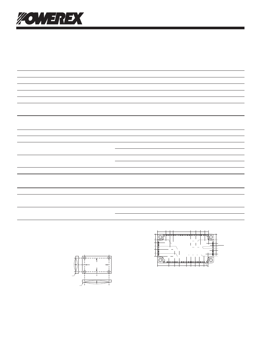
Refer to the figure to the right for chip location.
The heatsink thermal resistance should be measured just under the chips.
*7 Typical value is measured by using thermally conductive grease of λ = 0.9 [W/(m • K)].
*8 Baseplate (mounting side) flatness measurement points (X, Y) are shown in the figure below.
– :
CONC
A
VE
+ :
CONVEX
– : CONCAVE
X
Y
+ : CONVEX
MOUNTING
SIDE
MOUNTING SIDE
MOUNTING SIDE
1
2
3 4 5
6
7 8
9 10 11 12 13 14 15 16 17 18 19 20 21 22
53
54
55
56
57
58
59
60
61
30
29
28
27
26
25
24
23
52 51 50 49 48 47 46 45 44 43 42 41 40 39 38 37 36 35 34 33 32 31
0
0
17.5
20.0
18.1
31.2
32.6
47.0
48.0
15.2
LABEL SIDE
Each mark points to the center position of each chip.
Tr*P / Tr*N / TrBr (* = U/V/W): IGBT
Di*P / Di*N (* = U/V/W): FWDi
DiBr: Clamp Di
CR*P / CR*N (* = R/S/T): Conv Di
Th: NTC Thermistor
0
24.5
18.2
0
33.9
26.0
71
.8
82.9
93.0
102.3
46.8
36.4
62.9
72.1
81
.3
90.5
99.8
109.1
26.8
26.0
24.6
35.7
43.1
46.7
11
0.9
Tr
Br
Di
Br
Di
UN
Di
VN
Di
WN
Tr
UN
Tr
VN
Tr
WN
Tr
WP
Th
CR
RN
CR
SN
CR
TN
CR
RP
CR
SP
CR
TP
Di
WP
Di
VP
Tr
VP
Di
UP
Tr
UP