Vishay high power products, Electrical characteristics (t, 25 °c unless otherwise specified) – C&H Technology GA100NA60UP User Manual
Page 3: Switching characteristics (t
www.vishay.com
For technical questions, contact: [email protected]
Document Number: 94543
2
Revision: 13-May-08
GA100NA60UP
Vishay High Power Products
Insulated Gate Bipolar Transistor
(Ultrafast Speed IGBT), 50 A
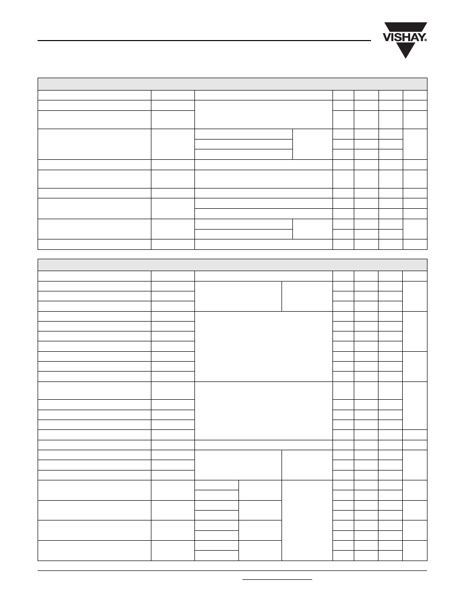
ELECTRICAL CHARACTERISTICS (T
J
= 25 °C unless otherwise specified)
PARAMETER SYMBOL
TEST
CONDITIONS
MIN.
TYP.
MAX.
UNITS
Collector to emitter breakdown voltage
V
(BR)CES
V
GE
= 0 V, I
C
= 250 µA
V
GE
= 0 V, I
C
= 1.0 mA
600
-
-
V
Temperature coeffecient of
breakdown voltage
ΔV
(BR)CES
/ΔT
J
-
0.36
-
V/°C
Collector to emitter saturation voltage
V
CE(on)
V
GE
= 15 V, I
C
= 50 A
See fig. 1, 4
-
1.49
2.1
V
V
GE
= 15 V, I
C
= 100 A
-
1.80
-
V
GE
= 15 V, I
C
= 50 A, T
J
= 150 °C
-
1.47
-
Gate threshold voltage
V
GE(th)
V
CE
= V
GE
, I
C
= 250 µA
3.0
-
6.0
Temperature coefficient of
threshold voltage
ΔV
GE(th)
/
ΔT
J
V
CE
= V
GE
, I
C
= 250 µA
-
- 7.6
-
mV/°C
Forward transconductance
g
fe
V
CE
= 100 V, I
C
= 50 A
34
52
-
S
Zero gate voltage collector current
I
CES
V
GE
= 0 V, V
CE
= 600 V
-
-
250
µA
V
GE
= 0 V, V
CE
= 600 V, T
J
= 150 °C
-
-
1.3
mA
Diode forward voltage drop
V
FM
I
C
= 50 A
See fig. 12
-
1.3
1.6
V
I
C
= 50 A, T
J
= 150 °C
-
1.16
1.3
Gate to emitter leakage current
I
GES
V
GE
= ± 20 V
-
-
± 100
nA
SWITCHING CHARACTERISTICS (T
J
= 25 °C unless otherwise specified)
PARAMETER SYMBOL
TEST
CONDITIONS
MIN.
TYP.
MAX.
UNITS
Total gate charge (turn-on)
Q
g
I
C
= 50 A
V
CC
= 400 V
V
GE
= 15 V
See fig. 7
-
430
640
nC
Gate emitter charge (turn-on)
Q
ge
-
48
72
Gate collector charge (turn-on)
Q
gc
-
130
190
Turn-on delay time
t
d(on)
T
J
= 25 °C
I
C
= 60 A, V
CC
= 480 V
V
GE
= 15 V, R
G
= 5.0
Ω
energy losses include “tail” and
diode reverse recovery
-
57
-
ns
Rise time
t
r
-
80
-
Turn-off delay time
t
d(off
)
-
240
-
Fall time
t
f
-
120
-
Turn-on switching loss
E
on
-
0.41
-
mJ
Turn-off switching loss
E
off
-
2.51
-
Total switching loss
E
ts
-
2.92
4.4
Turn-on delay time
t
d(on)
E
tot
T
J
= 150 °C
I
C
= 60 A, V
CC
= 480 V
V
GE
= 15 V, R
G
= 5.0
Ω
energy losses include “tail” and
diode reverse recovery
-
57
-
ns
Rise time
t
r
-
80
-
Turn-off delay time
t
d(off)
-
380
-
Fall time
t
f
-
170
-
Total switching loss
E
ts
-
4.78
-
mJ
Internal emitter inductance
L
E
-
2.0
-
nH
Input capacitance
C
ies
V
GE
= 0 V
V
CC
= 30 V
ƒ = 1.0 MHz
See fig. 6
-
7400
-
pF
Output capacitance
C
oes
-
730
-
Reverse transfer capacitance
C
res
-
90
-
Diode reverse recovery time
t
rr
T
J
= 25 °C
See fig. 13
I
F
= 50 A
V
R
= 200 V
dI/dt = 200 A/µs
-
90
140
ns
T
J
= 125 °C
-
120
180
Diode peak reverse recovery current
I
rr
T
J
= 25 °C
See fig. 14
-
7.3
11
A
T
J
= 125 °C
-
11
16
Diode reverse recovery charge
Q
rr
T
J
= 25 °C
See fig. 15
-
360
550
nC
T
J
= 125 °C
-
780
1200
Diode peak rate of fall recovery
during t
b
dI
(rec)M
/dt
T
J
= 25 °C
See fig. 16
-
370
-
A/µs
T
J
= 125 °C
-
220
-