Vishay semiconductors – C&H Technology VSKT570-18PbF User Manual
Page 6
Document Number: 93281
For technical questions, contact:
www.vishay.com
Revision: 05-May-11
5
This document is subject to change without notice.
THE PRODUCTS DESCRIBED HEREIN AND THIS DOCUMENT ARE SUBJECT TO SPECIFIC DISCLAIMERS, SET FORTH AT
www.vishay.com/doc?91000
VSKT570-18PbF
Thyristor/Thyristor
(SUPER MAGN-A-PAK Power Modules), 570 A
Vishay Semiconductors
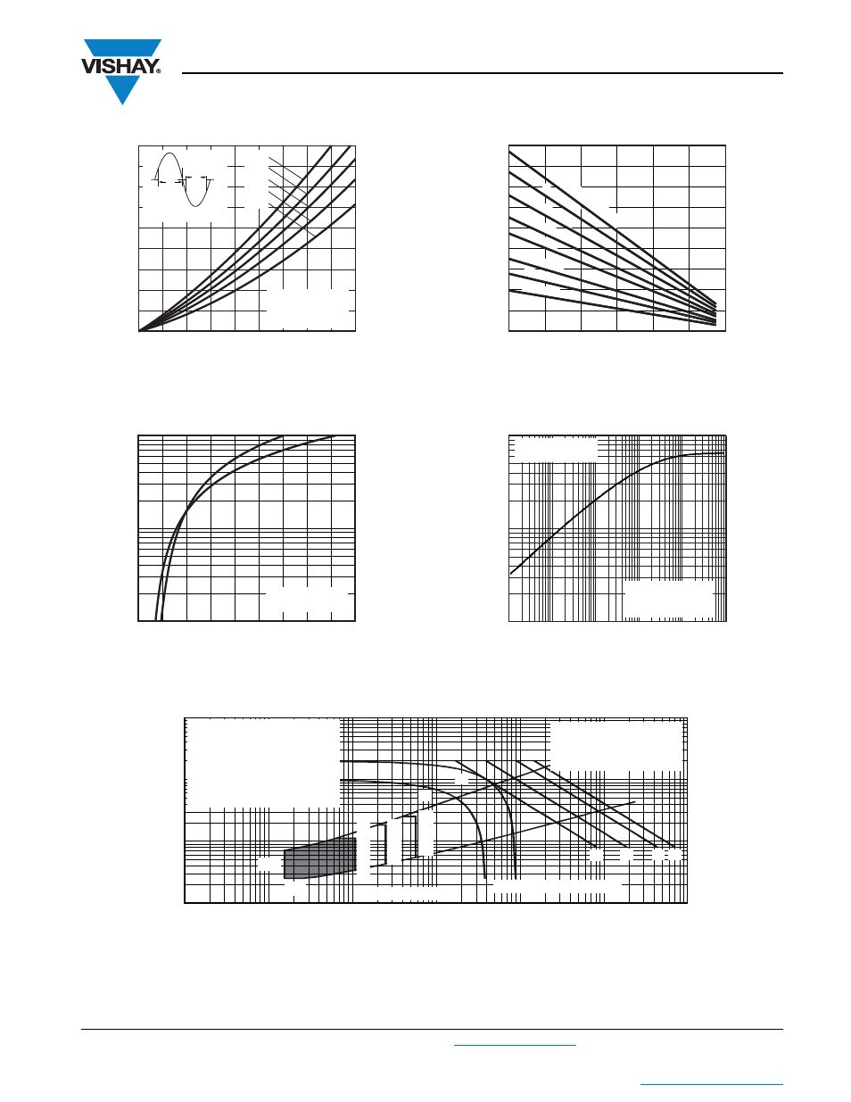
Fig. 7 - On-State Power Loss Characteristics
Fig. 8 - On-State Voltage Drop Characteristics
Fig. 9 - Thermal Impedance Z
thJC
Characteristics
Fig. 10 - Gate Characteristics
Maximum Total On-State
Power Loss (W)
Total RMS Output Current (A)
100 200 300 400 500 600
900
0
900
600
300
200
100
0
VSKT570... Series
per module
T
J
= 135 °C
Ш
Ш
Conduction angle
180°
120°
90°
60°
30°
700 800
700
800
500
400
Maximum Total On-State
Power Loss (W)
Maximum Allowable Ambient
Temperature (°C)
20
40
60
80
100
120
0
900
800
700
500
500
400
300
200
100
0
R
thSA
= 0.07 K/
W
0.09 K/
W
0.2 K/
W
0.12 K/
W
0.3 K/
W
0.4 K/
W
0.5 K/
W
0.6 K/W
Instantaneous On-
S
tate Current (A)
Instantaneous On-State Voltage (V)
1.0
1.5
2.0
5.0
0.5
10 000
1000
100
2.5
3.0
3.5
4.0
4.5
VSKT570... Series
per junction
0.001
0.01
0.1
0.001
0.01
0.1
1
10
Square Wave Pulse Duration (s)
Z
thJC
- Transient Thermal
Impe
d
ance (K/W)
100
Steady state value
R
thJC
= 0.065 K/W
(DC operation)
VSKT570... Series
per junction
0.1
1
10
100
0.001
Instantaneous Gate Current (A)
Instantaneous Gate Voltage (V)
0.01
0.1
1
10
100
1000
V
GD
I
GD
T
J
= 40 °C
T
J
= 25 °C
T
J
= 130 °C
(b)
(a)
Frequency limited by P
G(AV)
(1)
(2)
(3) (4)
Rectangular gate pulse
a) Recommended load line for
rated dI/dt: 20 V, 10
Ω;
t
r
≤ 1 µs
b) Recommended load line for
≤ 30 % rated dI/dt: 10 V, 10 Ω
t
r
≤ 1 µs
(1) P
GM
= 10 W, t
p
= 4 ms
(2) P
GM
= 20 W, t
p
= 2 ms
(3) P
GM
= 40 W, t
p
= 1 ms
(4) P
GM
= 60 W, t
p
= 0.66 ms
VSK.570... Series