Electrical characteristics @ t, 25°c (unless otherwise specified), Switching characteristics @ t – C&H Technology GA100TS60SF User Manual
Page 3: Thermal- mechanical specifications
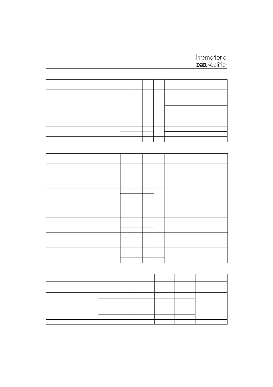
GA100TS60SF
Bulletin I27201 rev. A 01/06
T
J
Operating Junction Temperature Range
- 40
150
°C
T
STG
Storage Temperature Range
- 40
125
R
thJC
Junction-to-Case
per Switch
0.16
°C/ W
Per Diode
0.48
R
thCS
Case-to-Sink
Per Module
0.1
T
Mounting torque
Case to heatsink
4
Nm
Case to terminal 1, 2, 3
3
Weight
185
g
V
BRCES
Collector-to-Emitter Breakdown Voltage
600
V
V
GE
= 0V, I
C
= 1mA
V
CE(on)
Collector-to-Emitter Voltage
1.11
1.28
V
GE
= 15V, I
C
= 100A
1.39
I
C
= 200A
1.08
1.22
V
GE
= 15V, I
C
= 100A, T
J
= 125°C
V
GE(th)
Gate Threshold Voltage
3
6
I
C
= 0.25mA
I
CES
Collector-to-Emiter Leakage
1
mA
V
GE
= 0V, V
CE
= 600V
Current
10
V
GE
= 0V, V
CE
= 600V, T
J
= 125°C
V
F M
Diode Forward Voltage drop
1.44
1.96
V
I
C
= 100A, V
GE
= 0V
1.25
1.54
I
C
= 100A, V
GE
= 0V, T
J
= 125°C
I
GES
Gate-to-Emitter Leakage Current
± 250
nA
V
GE
= ± 20V
Electrical Characteristics @ T
J
= 25°C (unless otherwise specified)
Parameters
Min Typ Max Units Test Conditions
Q
g
Total Gate Charge
640
700
nC
I
C
= 100A
Q
ge
Gate-Emitter Charge
108
120
V
CC
= 400V
Q
gc
Gate-Collector Charge
230
300
V
GE
= 15V
t
r
Rise Time
0.45
µs
I
C
= 100A, V
CC
= 480V, V
GE
= 15V
t
f
Fall Time
1.0
R
g
= 15Ω
E
on
Turn-On Switching Energy
4
6
mJ
E
off
Turn-Off Switching Energy
23
29
E
ts
Total Switching Energy
27
35
E
on
Turn-On Switching Energy
6
12
mJ
I
C
= 100A, V
CC
= 480V, V
GE
= 15V
E
off
Turn-Off Switching Energy
35
40
R
g
= 15Ω
, T
J
= 125°C
E
ts
Total Switching Energy
41
52
C
ies
Input Capacitance
16250
pF
V
GE
= 0V
C
oes
Output Capacitance
1040
V
CC
= 30V
C
res
Reverse Transfer Capacitance
190
f = 1.0 MHz
t
rr
Diode Reverse Recovery Time
91
155
ns
I
F
= 50A, d
IF
/dt = 200A/µs
I
rr
Diode Peak Reverse Current
10.6
15
A
V
RR
= 200V
Q
rr
Diode Recovery Charge
500
900
nC
t
rr
Diode Reverse Recovery Time
180
344
ns
I
F
= 50A, d
IF
/dt = 200A/µs
I
rr
Diode Peak Reverse Current
17
20.5
A
V
RR
= 200V
Q
rr
Diode Recovery Charge
1633
2315
nC
T
J
= 125°C
Switching Characteristics @ T
J
= 25°C (unless otherwise specified)
Parameters
Min Typ Max Units Test Conditions
Thermal- Mechanical Specifications
Parameters
Min
Typ
Max
Units
Document Number: 93619
www.vishay.com
2