Vishay semiconductors – C&H Technology VS-GT175DA120U User Manual
Page 7
VS-GT175DA120U
www.vishay.com
Vishay Semiconductors
Revision: 02-Aug-12
6
Document Number: 93990
For technical questions within your region:
,
,
THIS DOCUMENT IS SUBJECT TO CHANGE WITHOUT NOTICE. THE PRODUCTS DESCRIBED HEREIN AND THIS DOCUMENT
ARE SUBJECT TO SPECIFIC DISCLAIMERS, SET FORTH AT
www.vishay.com/doc?91000
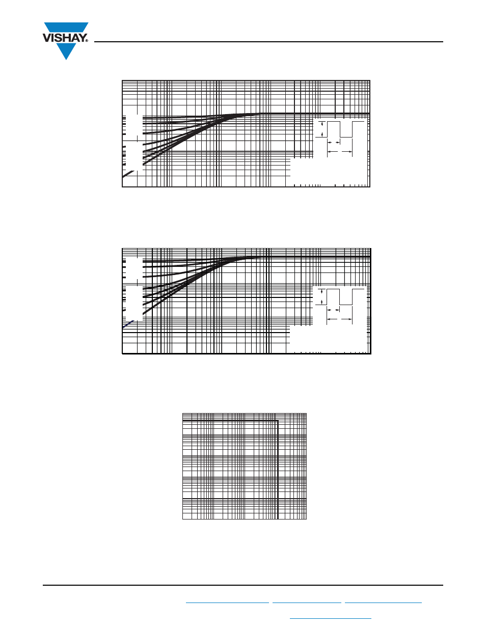
Fig. 16 - Maximum Thermal Impedance Z
thJC
Characteristics (IGBT)
Fig. 17 - Maximum Thermal Impedance Z
thJC
Characteristics (Diode)
Fig. 18 - IGBT Rverse Bias SOA, T
J
= 150 °C, V
GE
= 15 V
0.01
0.1
1
0.001
0.0001 0.001 0.01 0.1 1 10
P
DM
t
2
t
1
Notes:
1. Duty factor D = t
1
/t
2
2. Peak T
J
= P
DM
x Z
thJC
+ T
C
0.75
0.50
0.25
0.1
0.05
0.02
DC
Rectangular Pulse Duration (s)
Z
thJC
-
Thermal Impe
d
ance
Junction to Case (°C/W)
0.01
0.1
1
0.001
0.0001 0.001 0.01 0.1 1 10
Rectangular Pulse Duration (s)
Z
thJC
-
Thermal Impe
d
ance
Junction to Case (°C/W)
0.75
0.50
0.25
0.1
0.05
0.02
DC
P
DM
t
2
t
1
Notes:
1. Duty factor D = t
1
/t
2
2. Peak T
J
= P
DM
x Z
thJC
+ T
C
I
C
(A)
V
CE
(V)
1
10
100
1000
10 000
0.01
0.1
1
1000
10
100