Vishay semiconductors – C&H Technology VSKE91.. Series User Manual
Page 4
Document Number: 94627
For technical questions, contact:
www.vishay.com
Revision: 09-Mar-11
3
This datasheet is subject to change without notice.
THE PRODUCT DESCRIBED HEREIN AND THIS DATASHEET ARE SUBJECT TO SPECIFIC DISCLAIMERS, SET FORTH AT
www.vishay.com/doc?91000
VSKD91.., VSKC91.., VSKJ91.., VSKE91.. Series
ADD-A-PAK Generation VII
Power Modules Standard Diodes, 100 A
Vishay Semiconductors
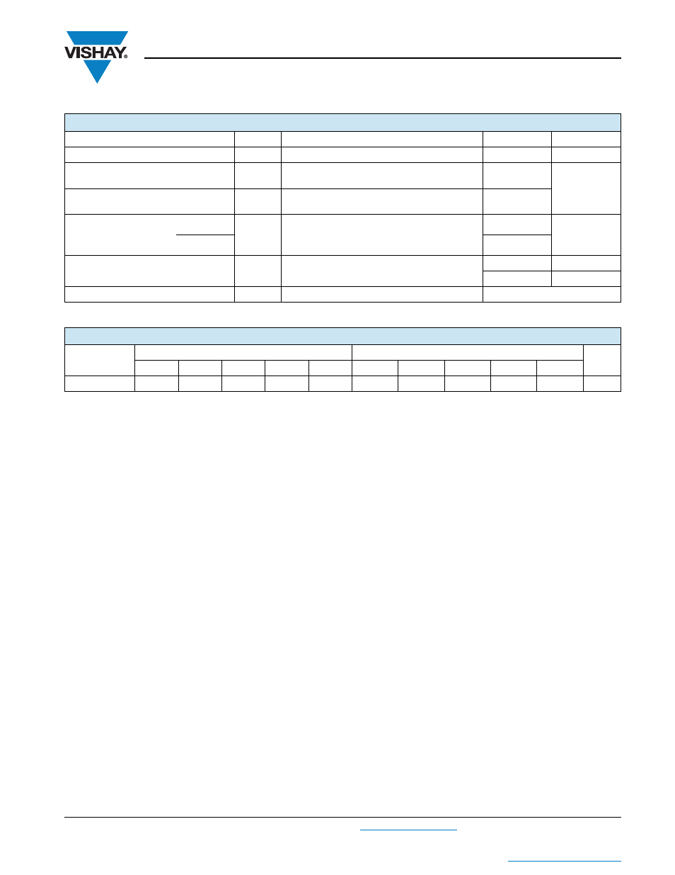
Note
• Table shows the increment of thermal resistance R
thJC
when devices operate at different conduction angles than DC
THERMAL AND MECHANICAL SPECIFICATIONS
PARAMETER
SYMBOL
TEST CONDITIONS
VALUES
UNITS
Junction and storage temperature range
T
J
, T
Stg
- 40 to 150
°C
Maximum internal thermal resistance,
junction to case per leg
R
thJC
DC operation
0.22
°C/W
Typical thermal resistance,
case to heatsink per module
R
thCS
Mounting surface flat, smooth and greased
0.1
Mounting torque ± 10 %
to heatsink
A mounting compound is recommended and the
torque should be rechecked after a period of
3 hours to allow for the spread of the compound.
4
Nm
busbar
3
Approximate weight
75
g
2.7
oz.
Case style
JEDEC
ADD-A-PAK Gen. VII (TO-240AA)
R CONDUCTION PER JUNCTION
DEVICES
SINE HALF WAVE CONDUCTION
RECTANGULAR WAVE CONDUCTION
UNITS
180°
120°
90°
60°
30°
180°
120°
90°
60°
30°
VSK.91
0.057
0.068
0.087
0.12
0.177
0.045
0.073
0.093
0.123
0.178
°C/W