Vishay semiconductors, Electrical specifications, Voltage ratings – C&H Technology VSKN26.. Series User Manual
Page 3: On-state conduction
www.vishay.com
For technical questions within your region, please contact one of the following:
Document Number: 94629
2
,
,
Revision: 17-May-10
VSKT26.., VSKH26.., VSKL26.., VSKN26.. Series
Vishay Semiconductors
ADD-A-PAK Generation VII Power Modules
Thyristor/Diode and Thyristor/Thyristor, 27 A
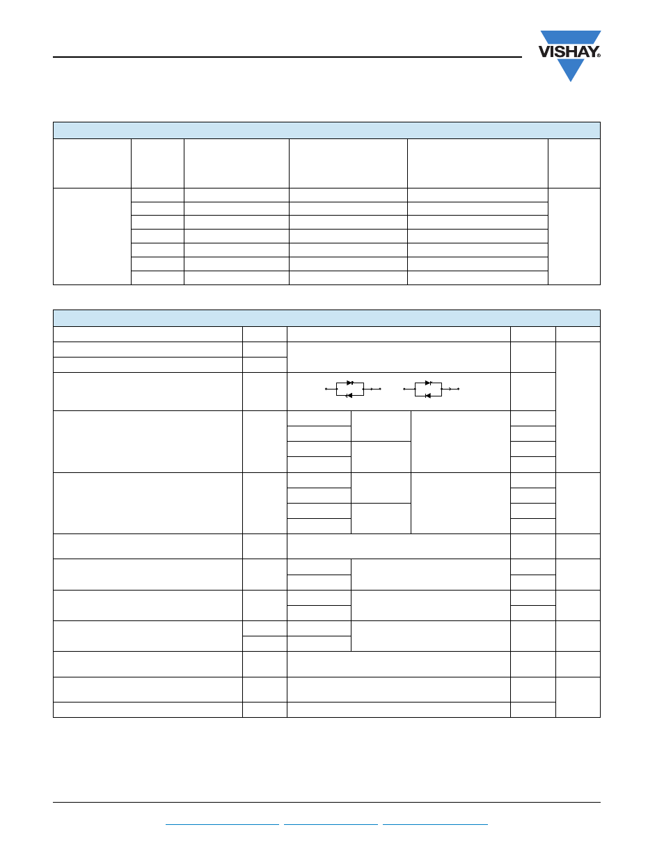
ELECTRICAL SPECIFICATIONS
Notes
(1)
I
2
t for time t
x
= I
2
√t x √t
x
(2)
Average power = V
T(TO)
x I
T(AV)
+ r
t
x (I
T(RMS)
)
2
(3)
16.7 % x
π x I
AV
< I <
π x I
AV
(4)
I >
π x I
AV
VOLTAGE RATINGS
TYPE NUMBER
VOLTAGE
CODE
V
RRM
, MAXIMUM
REPETITIVE PEAK
REVERSE VOLTAGE
V
V
RSM
, MAXIMUM
NON-REPETITIVE PEAK
REVERSE VOLTAGE
V
V
DRM
, MAXIMUM REPETITIVE
PEAK OFF-STATE VOLTAGE,
GATE OPEN CIRCUIT
V
I
RRM,
I
DRM
AT 125 °C
mA
VSK.26
04
400
500
400
15
06
600
700
600
08
800
900
800
10
1000
1100
1000
12
1200
1300
1200
14
1400
1500
1400
16
1600
1700
1600
ON-STATE CONDUCTION
PARAMETER
SYMBOL
TEST CONDITIONS
VALUES
UNITS
Maximum average on-state current (thyristors)
I
T(AV)
180° conduction, half sine wave,
T
C
= 85 °C
27
A
Maximum average forward current (diodes)
I
F(AV)
Maximum continuous RMS on-state current,
as AC switch
I
O(RMS)
60
Maximum peak, one-cycle non-repetitive
on-state or forward current
I
TSM
or
I
FSM
t = 10 ms
No voltage
reapplied
Sinusoidal
half wave,
initial T
J
= T
J
maximum
400
t = 8.3 ms
420
t = 10 ms
100 % V
RRM
reapplied
335
t = 8.3 ms
350
Maximum I
2
t for fusing
I
2
t
t = 10 ms
No voltage
reapplied
Initial T
J
= T
J
maximum
800
A
2
s
t = 8.3 ms
730
t = 10 ms
100 % V
RRM
reapplied
560
t = 8.3 ms
510
Maximum I
2
√t for fusing
I
2
√t
(1)
t = 0.1 ms to 10 ms, no voltage reapplied
T
J
= T
J
maximum
8000
A
2
√s
Maximum value or threshold voltage
V
T(TO)
(2)
Low level
(3)
T
J
= T
J
maximum
0.86
V
High level
(4)
1.09
Maximum value of on-state
slope resistance
r
t
(2)
Low level
(3)
T
J
= T
J
maximum
9.58
m
Ω
High level
(4)
7.31
Maximum peak on-state or forward voltage
V
TM
I
TM
=
π x I
T(AV)
T
J
= 25 °C
1.65
V
V
FM
I
FM
=
π x I
F(AV)
Maximum non-repetitive rate of rise of
turned on current
dI/dt
T
J
= 25 °C, from 0.67 V
DRM
,
I
TM
=
π x I
T(AV)
, I
g
= 500 mA, t
r
< 0.5 μs, t
p
> 6 μs
150
A/μs
Maximum holding current
I
H
T
J
= 25 °C, anode supply = 6 V,
resistive load, gate open circuit
200
mA
Maximum latching current
I
L
T
J
= 25 °C, anode supply = 6 V, resistive load
400
or
I
(RMS)
I
(RMS)