Vishay semiconductors, Electrical specifications (t, 25 °c unless otherwise specified) – C&H Technology VS-GA400TD60S User Manual
Page 3: Switching characteristics (t
www.vishay.com
For technical questions, contact:
Document Number: 93363
2
Revision: 31-May-11
This document is subject to change without notice.
THE PRODUCTS DESCRIBED HEREIN AND THIS DOCUMENT ARE SUBJECT TO SPECIFIC DISCLAIMERS, SET FORTH AT
www.vishay.com/doc?91000
GA400TD60S
Vishay Semiconductors
Dual INT-A-PAK Low Profile "Half-Bridge"
(Standard Speed IGBT), 400 A
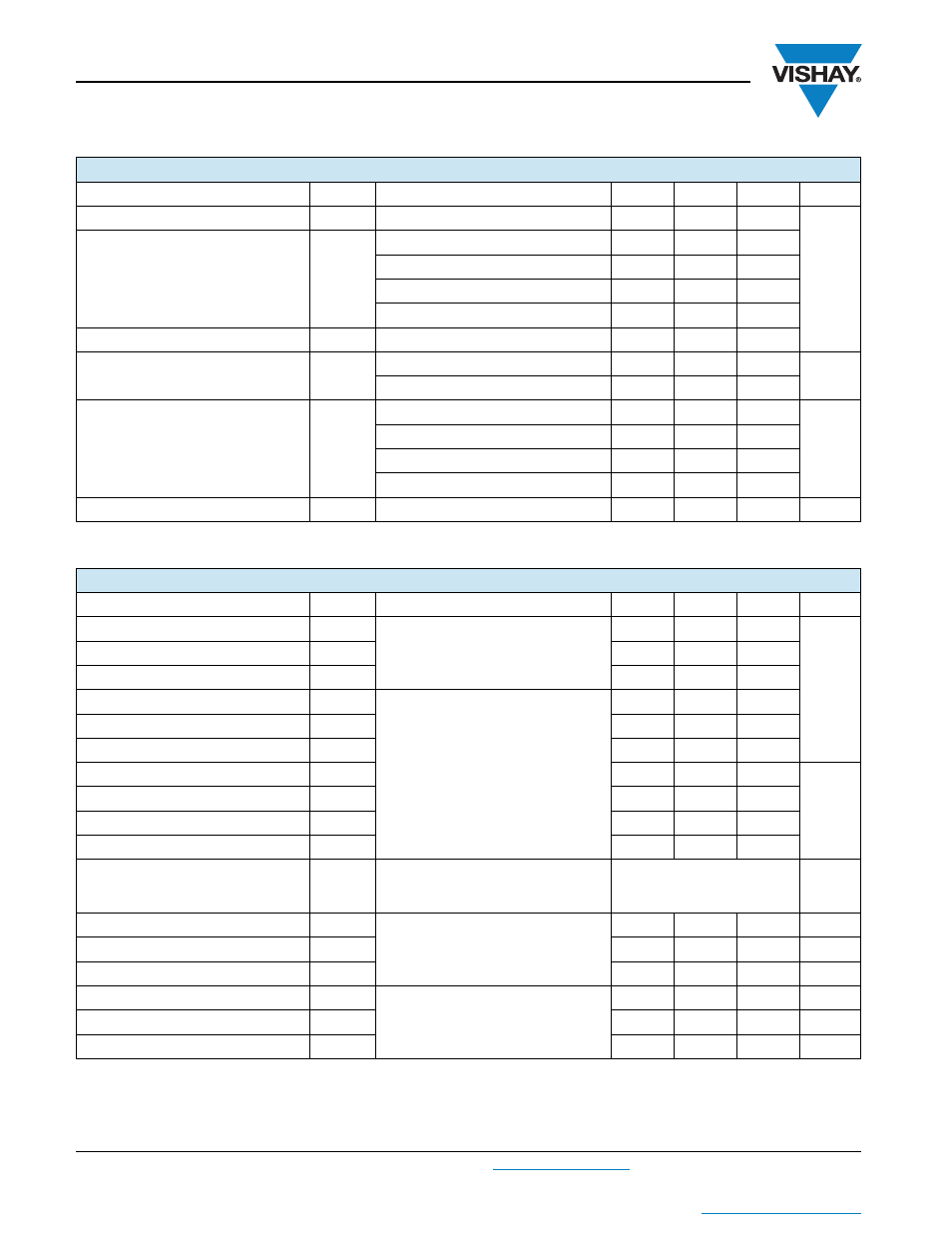
ELECTRICAL SPECIFICATIONS (T
J
= 25 °C unless otherwise specified)
PARAMETER SYMBOL
TEST
CONDITIONS MIN.
TYP.
MAX.
UNITS
Collector to emitter breakdown voltage
V
BR(CES)
V
GE
= 0 V, I
C
= 500 μA
600
-
-
V
Collector to emitter voltage
V
CE(on)
V
GE
= 15 V, I
C
= 300 A
-
1.14
1.35
V
GE
= 15 V, I
C
= 400 A
-
1.24
1.52
V
GE
= 15 V, I
C
= 300 A, T
J
= 125 °C
-
1.08
1.29
V
GE
= 15 V, I
C
= 400 A, T
J
= 125 °C
-
1.21
1.5
Gate threshold voltage
V
GE(th)
V
CE
= V
GE
, I
C
= 250 μA
3.0
4.6
6.3
Collector to emitter leakage current
I
CES
V
GE
= 0 V, V
CE
= 600 V
-
0.075
1
mA
V
GE
= 0 V, V
CE
= 600 V, T
J
= 125 °C
-
1.8
10
Diode forward voltage drop
V
FM
I
FM
= 300 A
-
1.48
1.75
V
I
FM
= 400 A
-
1.63
1.98
I
FM
= 300 A, T
J
= 125 °C
-
1.50
1.77
I
FM
= 400 A, T
J
= 125 °C
-
1.70
2.04
Gate to emitter leakage current
I
GES
V
GE
= ± 20 V
-
-
± 200
nA
SWITCHING CHARACTERISTICS (T
J
= 25 °C unless otherwise specified)
PARAMETER SYMBOL
TEST
CONDITIONS MIN.
TYP.
MAX.
UNITS
Turn-on switching loss
E
on
I
C
= 400 A, V
CC
= 360 V, V
GE
= 15 V,
R
g
= 1.5
, L = 500 μH, T
J
= 25 °C
-
8.5
-
mJ
Turn-off switching loss
E
off
-
113
-
Total switching loss
E
tot
-
121.5
-
Turn-on switching loss
E
on
I
C
= 400 A, V
CC
= 360 V, V
GE
= 15 V,
R
g
= 1.5
, L = 500 μH, T
J
= 125 °C
-
21
-
Turn-off switching loss
E
off
-
163
-
Total switching loss
E
tot
-
184
-
Turn-on delay time
t
d(on)
-
532
-
ns
Rise time
t
r
-
377
-
Turn-off delay time
t
d(off)
-
496
-
Fall time
t
f
-
1303
-
Reverse bias safe operating area
RBSOA
T
J
= 150 °C, I
C
= 1000 A, V
CC
= 400 V,
V
P
= 600 V, R
g
= 22
V
GE
= 15 V to 0 V,
L = 500 μH
Fullsquare
Diode reverse recovery time
t
rr
I
F
= 300 A, dI
F
/dt = 500 A/μs,
V
CC
= 400 V, T
J
= 25 °C
-
150
179
ns
Diode peak reverse current
I
rr
-
43
59
A
Diode recovery charge
Q
rr
-
3.9
6.3
μC
Diode reverse recovery time
t
rr
I
F
= 300 A, dI
F
/dt = 500 A/μs,
V
CC
= 400 V, T
J
= 125 °C
-
236
265
ns
Diode peak reverse current
I
rr
-
64
80
A
Diode recovery charge
Q
rr
-
8.6
11.1
μC