Electrical characteristics, t, 25°c unless otherwise specified, Brake part igbt/clampdi – C&H Technology CM75MX-12A User Manual
Page 5: Converter part, Ntc thermistor part
CM75MX-12A
NX-Series CIB Module
(3Ø Converter + 3Ø Inverter + Brake)
75 Amperes/600 Volts
Powerex, Inc., 173 Pavilion Lane, Youngwood, Pennsylvania 15697 (724) 925-7272 www.pwrx.com
4
Rev. 11/11
Electrical Characteristics,
T
j
= 25°C unless otherwise specified
Characteristics
Symbol
Test Conditions
Min.
Typ.
Max.
Units
Brake Part IGBT/ClampDi
Collector Cutoff Current
I
CES
V
CE
= V
CES
, V
GE
= 0V
—
—
1.0
mA
Gate Leakage Current
I
GES
V
GE
= V
GES
, V
CE
= 0V
—
—
0.5
µA
Gate-Emitter Threshold Voltage
V
GE(th)
I
C
= 5mA, V
CE
= 0V
5
6
7
Volts
Collector-Emitter Saturation Voltage
V
CE(sat)
T
j
= 25°C, I
C
= 50A, V
GE
= 15V
*5
— 1.7 2.1 Volts
T
j
= 125°C, I
C
= 50A, V
GE
= 15V
*5
— 1.9 — Volts
I
C
= 50A, V
GE
= 15V, Chip
—
1.6
—
Volts
Input Capacitance
C
ies
— — 9.3 nF
Output Capacitance
C
oes
V
CE
= 10V, V
GE
= 0V
—
—
1.0
nF
Reverse Transfer Capacitance
C
res
— — 0.3 nF
Total Gate Charge
Q
G
V
CC
= 300V, I
C
= 50A, V
GE
= 15V
—
200
—
nC
Internal Gate Resistance
r
g
T
C
= 25°C
—
0
—
Ω
Repetitive Reverse Current
I
RRM
V
R
= V
RRM
— — 1.0 mA
Forward Voltage Drop
V
F
T
j
= 25°C, I
F
= 50A
*5
— 2.0 2.8 Volts
T
j
= 125°C, I
F
= 50A
*5
— 1.95 — Volts
I
F
= 50A, Chip
—
1.9
—
Volts
External Gate Resistance
R
G
13 — 125 Ω
Converter Part
Repetitive Peak Reverse Current
I
RRM
V
R
= V
RRM
, T
j
= 150°C
—
—
20
mA
Forward Voltage Drop
V
F
I
F
= 75A
*5
— 1.2 1.6 Volts
NTC Thermistor Part
Zero Power Resistance
R
25
T
C
= 25°C
*4
4.85 5.00 5.15 kΩ
Deviation of Resistance
∆R/R R
100
= 493Ω, T
C
= 100°C
*4
-7.3 — +7.8 %
B Constant
B
(25/50)
Approximate by Equation
*6
— 3375 — K
Power Dissipation
P
25
T
C
= 25°C
*4
— — 10 mW
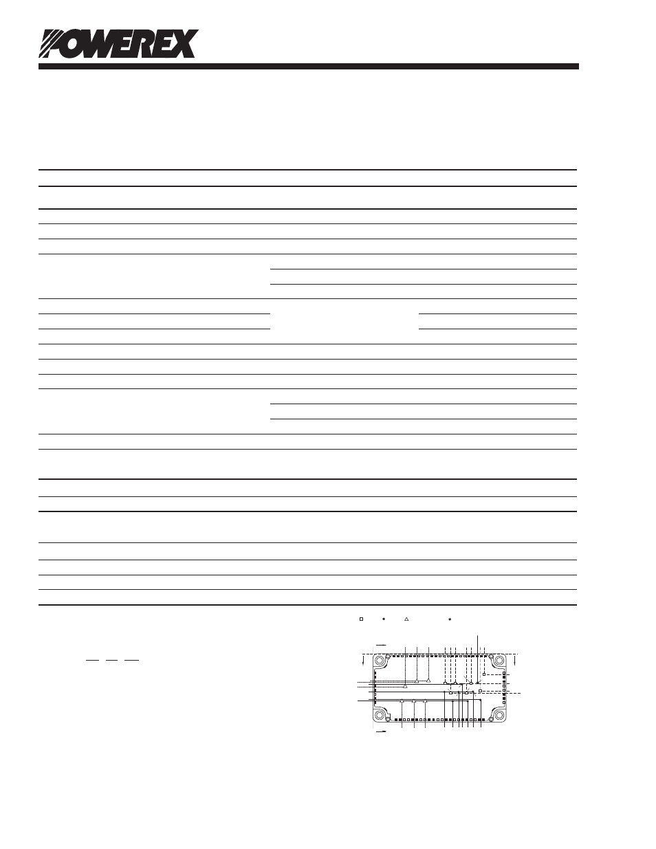
*4 Case temperature (T
C
) and heatsink temperature (T
s
) is measured on the surface
(mounting side) of the baseplate and the heatsink side just under the chips.
Refer to the figure to the right for chip location.
The heatsink thermal resistance should be measured just under the chips.
*5 Pulse width and repetition rate should be such as to cause negligible temperature rise.
*6 B
(25/50)
= In(
R
25
)/(
1
–
1
)
R
50
T
25
T
50
R
25
; Resistance at Absolute Temperature T
25
[K]; T
25
= 25 [°C] + 273.15 = 298.15 [K]
R
50
; Resistance at Absolute Temperature T
50
[K]; T
50
= 50 [°C] + 273.15 = 323.15 [K]
0
0
0
0
1
2
3 4 5
6
7 8
9 10 11 12 13 14 15 16 17 18 19 20 21 22
53
54
55
56
57
58
59
60
61
30
29
28
27
26
25
24
23
52 51 50 49 48 47 46 45 44 43 42 41 40 39 38 37 36 35 34 33 32 31
V
P
W
P
W
N
Br
V
N
U
N
U
P
TN
SN
RN
RP SP TP
64.2
73.0
77
.8
81
.4
86.1 91
.4
97
.9
27.6
34.7
41.2
42.0
25.5
42.9
26.5
29.5
26.6
37
.0
47
.4
29.5
39.9
50.3
65.5
Th
95.5
10
1.
2
89.6
98.2
74.6
71
.0
17.8
27.1
33.6 35.2
Dimensions in mm (Tolerance: ±1mm)
IGBT FWDi Converter Diode NTC Thermistor
Chip Location (Top View)
84.6
U
P
V
P
W
P
W
N
V
N
U
N
Br