Absolute maximum ratings, t, 25°c unless otherwise specified, Inverter part igbt/fwdi – C&H Technology CM75MX-12A User Manual
Page 3: Brake part igbt/clampdi, Converter part convdi, Module
CM75MX-12A
NX-Series CIB Module
(3Ø Converter + 3Ø Inverter + Brake)
75 Amperes/600 Volts
Powerex, Inc., 173 Pavilion Lane, Youngwood, Pennsylvania 15697 (724) 925-7272 www.pwrx.com
2
Rev. 11/11
Absolute Maximum Ratings,
T
j
= 25°C unless otherwise specified
Characteristics
Symbol CM75MX-12A Units
Inverter Part IGBT/FWDi
Collector-Emitter Voltage (G-E Short)
V
CES
600 Volts
Gate-Emitter Voltage (C-E Short)
V
GES
±20 Volts
Collector Current (DC, T
C
= 70°C)
*2,*4
I
C
75 Amperes
Collector Current (Pulse)
*3
I
CRM
150 Amperes
Total Power Dissipation (T
C
= 25°C)
*2,*4
P
tot
280 Watts
Emitter Current
*2
I
E
*1
75 Amperes
Emitter Current (Pulse)
*3
I
ERM
*1
150 Amperes
Brake Part IGBT/ClampDi
Collector-Emitter Voltage (G-E Short)
V
CES
600 Volts
Gate-Emitter Voltage (C-E Short)
V
GES
±20 Volts
Collector Current (DC, T
C
= 97°C)
*2,*4
I
C
50 Amperes
Collector Current (Pulse)
*3
I
CRM
100 Amperes
Total Power Dissipation (T
C
= 25°C)
*2,*4
P
tot
280 Watts
Repetitive Peak Reverse Voltage
V
RRM
600 Volts
Forward Current (T
C
= 25°C)
*2
I
F
50 Amperes
Forward Current (Pulse)
*3
I
FRM
100 Amperes
Converter Part ConvDi
Repetitive Peak Reverse Voltage
V
RRM
800 Volts
Recommended AC Input Voltage
E
a
220 Volts
DC Output Current (3-Phase Full Wave Rectifying, f = 60Hz,T
C
= 125°C)
*2,*4
I
O
75 Amperes
Surge Forward Current (Sine Half-wave 1 Cycle Peak Value, f = 60Hz, Non-repetitive)
I
FSM
750 Amperes
Current Square Time (Value for One Cycle of Surge Current)
I
2
t 2340 A
2
s
Module
Isolation Voltage (Charged Part to Baseplate, RMS, f = 60Hz, AC 1 min.)
V
ISO
2500 Volts
Junction Temperature
T
j
-40 ~ +150
°C
Storage Temperature
T
stg
-40 ~ +125
°C
*1 Represent ratings and characteristics of the anti-parallel, emitter-to-collector free wheeling diode (FWDi).
*2 Junction temperature (T
j
) should not increase beyond maximum junction temperature (T
j(max)
) rating.
*3 Pulse width and repetition rate should be such that device junction temperature (T
j
) does not exceed T
j(max)
rating.
*4 Case temperature (T
C
) and heatsink temperature (T
s
) is measured on the surface (mounting side) of the baseplate
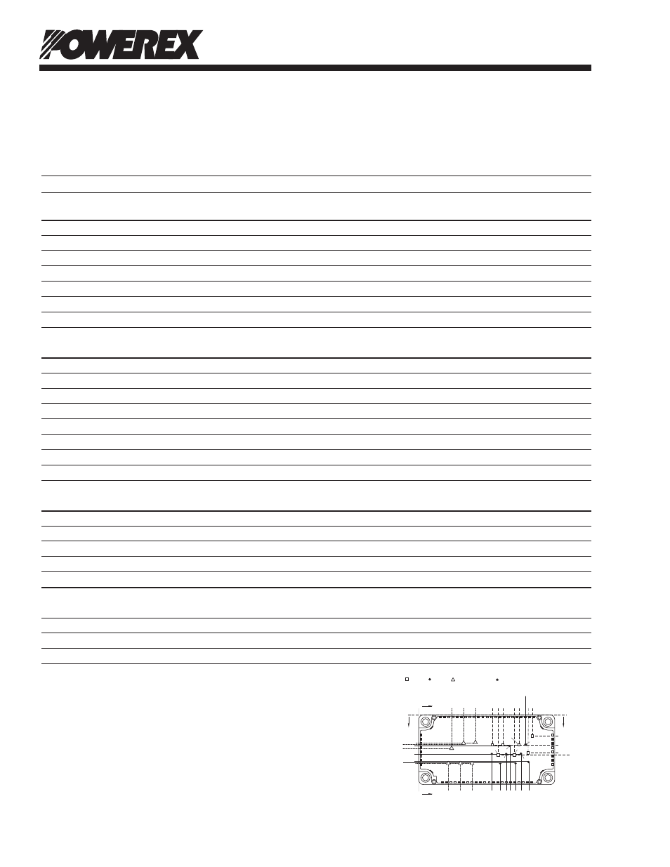
and the heatsink side just under the chips. Refer to the figure to the right for chip location.
The heatsink thermal resistance should be measured just under the chips.
0
0
0
0
1
2
3 4 5
6
7 8
9 10 11 12 13 14 15 16 17 18 19 20 21 22
53
54
55
56
57
58
59
60
61
30
29
28
27
26
25
24
23
52 51 50 49 48 47 46 45 44 43 42 41 40 39 38 37 36 35 34 33 32 31
V
P
W
P
W
N
Br
V
N
U
N
U
P
TN
SN
RN
RP SP TP
64.2
73.0
77
.8
81
.4
86.1 91
.4
97
.9
27.6
34.7
41.2
42.0
25.5
42.9
26.5
29.5
26.6
37
.0
47
.4
29.5
39.9
50.3
65.5
Th
95.5
10
1.
2
89.6
98.2
74.6
71
.0
17.8
27.1
33.6 35.2
Dimensions in mm (Tolerance: ±1mm)
IGBT FWDi Converter Diode NTC Thermistor
Chip Location (Top View)
84.6
U
P
V
P
W
P
W
N
V
N
U
N
Br