Acnodes PCH 3582 User Manual
Page 20
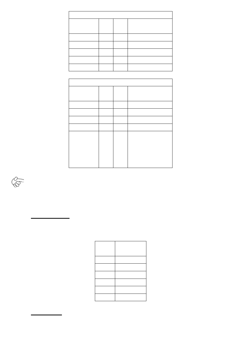
COM2,COM3,COM4,COM5 Signal Name:
Signal
Name
Pin# Pin# Signal Name
DCD
1
2
RXD
TXD
3
4
DTR
Ground
5
6
DSR
RTS
7
8
CTS
RI
9
10
NC
COM6 Signal Name:
Signal
Name
Pin# Pin# Signal Name
DCD
1
2
RXD
TXD
3
4
DTR
Ground
5
6
DSR
RTS
7
8
CTS
RI
9
10
JCOM6 Setting:
Pin1-2 : 5V
(Default)
Pin2-3:12V
(option)
Note:
COM3 port is controlled by pins No.7~10 of JCOM. For details, please refer to
description of JCOM and COM33 BIOS Setup.
14. KB/MS:
(2.0mm Pitch 1x6 box Pin Header), PS/2 keyboard and mouse port, the
port can be connected to PS/2 keyboard or mouse via a dedicated cable for direct
used.
Pin#
Signal
Name
1
KBDATA
2
MSDATA
3
Ground
4
+5V
5
KBCLK
6
MSCLK
15. USB1/2
:
(Double stack USB type A), Rear USB connector, it provides up to 4