Signal groups description – Texas Instruments TMS320C6712D User Manual
Page 18

TMS320C6712D
FLOATINGĆPOINT DIGITAL SIGNAL PROCESSOR
SPRS293A − OCTOBER 2005 − REVISED NOVEMBER 2005
18
POST OFFICE BOX 1443
•
HOUSTON, TEXAS 77251−1443
signal groups description
TRST
EXT_INT7‡
IEEE Standard
1149.1
(JTAG)
Emulation
Reserved
Reset and
Interrupts
Control/Status
TDI
TDO
TMS
TCK
EMU0
EMU1
NMI
EXT_INT6‡
EXT_INT5‡
EXT_INT4‡
RESET
Clock/PLL
CLKOUT3
CLKMODE0
CLKOUT2†
EMU2
EMU3
EMU4
EMU5
CE3
ECLKOUT
ED[15:0]
CE2
CE1
CE0
EA[21:2]
BE1
BE0
AOE/SDRAS/SSOE
AWE/SDWE/SSWE
ARDY
Data
Memory Map
Space Select
Address
Byte Enables
16
20
Memory
Control
EMIF (16-bit)
(External Memory Interface)
ECLKIN
HOLD
HOLDA
BUSREQ
Bus
Arbitration
ARE/SDCAS/SSADS
BIG/LITTLE
ENDIAN
BOOTMODE
EMIFBE§
BOOTMODE1
BOOTMODE0
† The CLKOUT2 pin is multiplexed with the GP[2] pin. Default function is CLKOUT2. To use this pin as GPIO, the GP2EN bit in
the GPEN register and the GP2DIR bit in the GPDIR register must be properly configured.
‡ The external interrupts (EXT_INT[7−4]) go through the general-purpose input/output (GPIO) module. When used as interrupt
inputs, the GP[7−4] pins must be configured as inputs (via the GPDIR register) and enabled (via the GPEN register) in addition
to enabling the interrupts in the interrupt enable register (IER).
§ This pin functions as the Big Endian mode correctness and is used when Big Endian mode is selected (LENDIAN = 0)
RSV
RSV
RSV
RSV
•
•
•
CLKIN
PLLHV
LENDIAN
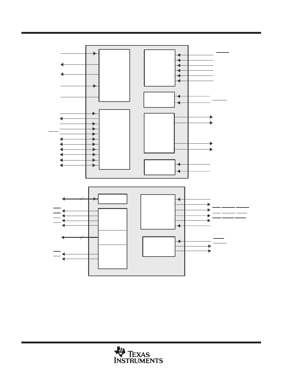
Figure 3. CPU (DSP Core) and Peripheral Signals
