Application headers – Renesas RSKM16C6NK User Manual
Page 22
9.2. Application Headers
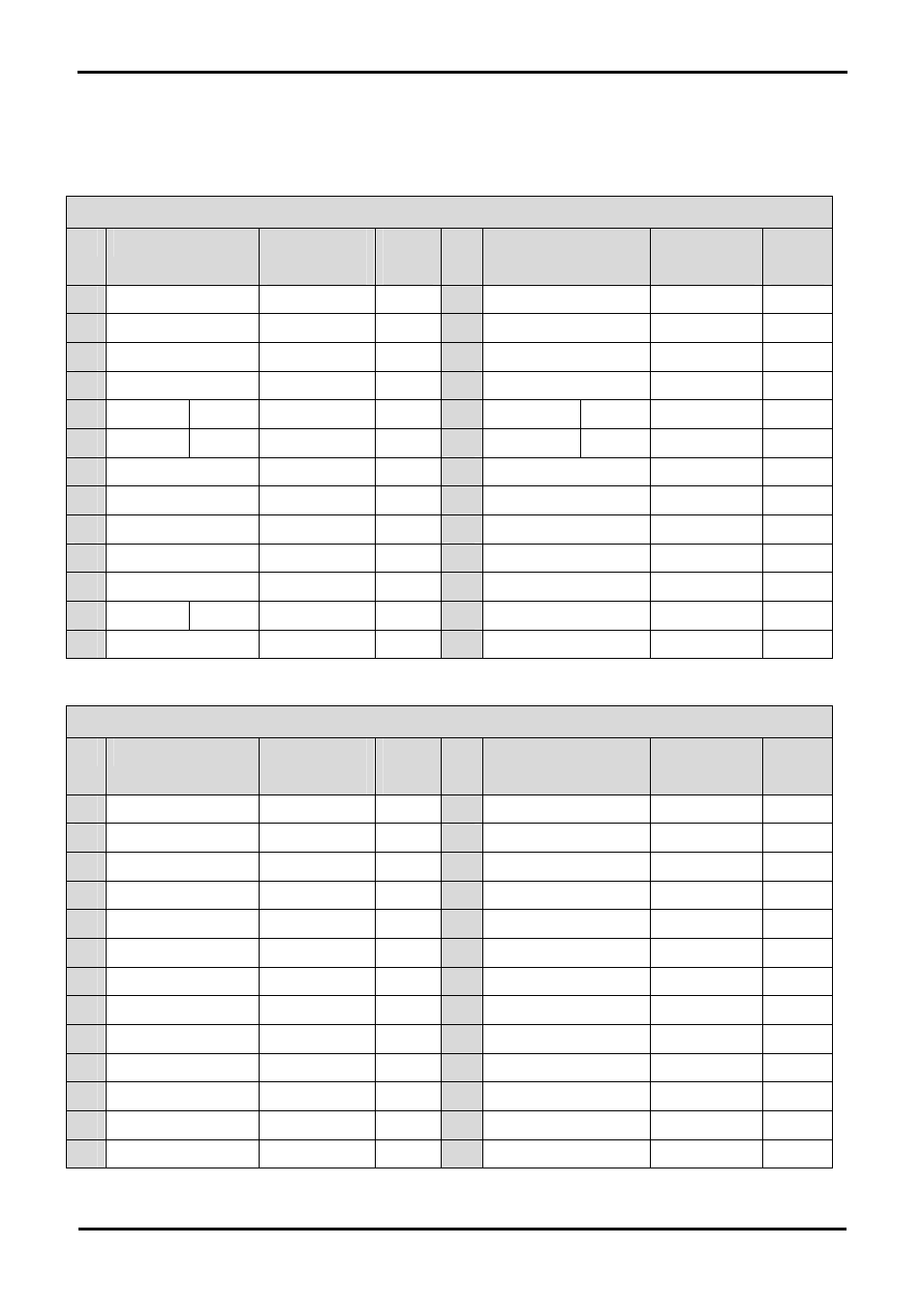
Table 9-5 and Table 9-6 below show the standard application connections. * Marked pins are subject to option links.
JA1
Pin Generic Header Name
RSK Signal
Name
Device
Pin
Pin
Header Name
RSK Signal
Name
Device
Pin
1
Regulated Supply 1
5V
2
Regulated Supply 1
GROUND
3
Regulated Supply 2
3V3
4
Regulated Supply 2
GROUND
5 Analogue
Supply
AVcc
97
6 Analogue
Supply
AVss
94
7 Analogue
Reference AVref
96
8 ADTRG
ADTRG
98
9 ADC0
I0
ADPot_AN0* 95
10 ADC1
I1
AN1
93
11 ADC2
I2
AN2
92
12 ADC3
I3
AN3
91
13 DAC0
DA0
2
14 DAC1
DA1
1
15 IOPort
A8_IO_0
61
16 IOPort
A9_IO_1
59
17 IOPort
A10_IO_2
58
18 IOPort
A11_IO_3
57
19 IOPort
A12_IO_4
56
20 IOPort
A13_IO_5
55
21 IOPort
A14_IO_6
54
22 IOPort
A15_IO_7
53
23 Interrupt IRQAEC D13_INT3
73
24
I²C Bus - (3rd pin)
NC
-
25 I²C
Bus
IIC_SDA*
28
26 I²C
Bus
IIC_SCL*
27
Table 9-5: JA1 Standard Generic Header
JA2
Pin
Header Name
RSK Signal
Name
Device
Pin
Pin
Header Name
RSK Signal
Name
Device
Pin
1 Reset
RESn
10
2
External Clock Input
EXTAL
-
3 Interrupt
NMIn
15
4
Regulated Supply 1
Vss1
5 SPARE
-
-
6 Serial
Port
TxD0
33
7 Interrupt
INT0
18
8
Serial Port
RxD0
34
9
Interrupt INT1
17
10 Serial
Port
CLK0
35
11
Motor control
UD
40
12
Serial Port Handshake
CTSRTS
36
13 Motor
control
Up*
20
14 Motor
control
Un*
19
15 Output
Vp*
26
16 Motor
control
Vn
25
17 Input
Wp*
24
18 Motor
control
Wn*
23
19 Output
TA2OUT*
23
20 Output
TA4OUT
20
21 Input
TA2IN*
20
22 Input
TA4IN
19
23 Open
drain
INT2
16
24 Tristate
Control
TRSTn
41
25 SPARE
-
26 SPARE
-
Table 9-6: JA2 Standard Generic Header
20