6 port i/o timing – Renesas MCU Board for 4513/4514 Group MCUs M34514T-MCU User Manual
Page 31
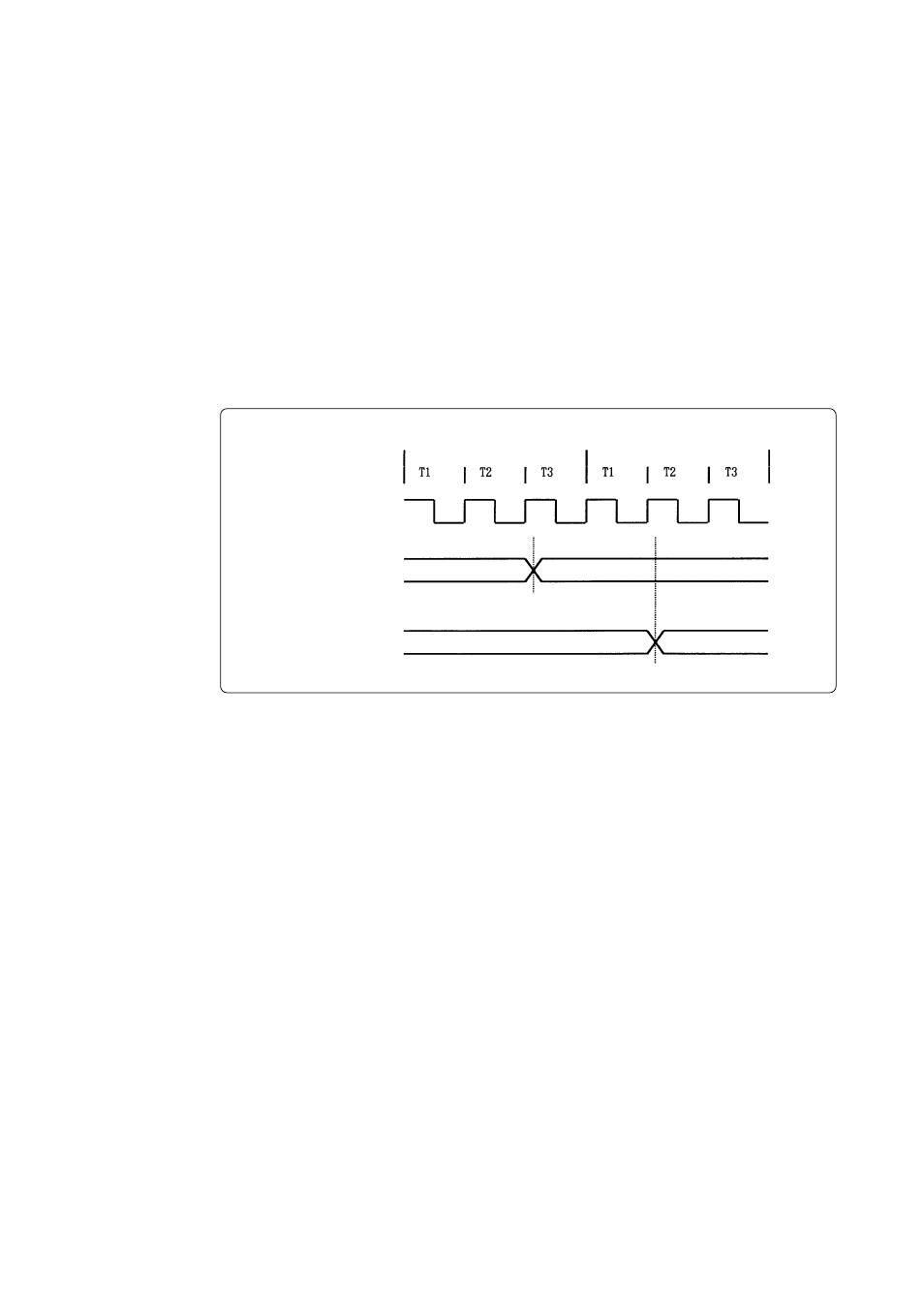
( 31 / 42 )
Figure 5.2 P0, P1 and D port output timings
5.6 Port I/O Timing
(1) Port input timing
Port input timings are the same as with the actual MCUs.
(2) Port output timing
When using the M34514T-MCU, output timings are different from those of the actual MCUs for
the following ports that are configured with port emulation circuits:
• Ports P0
0
to P0
3
• Ports P1
0
to P1
3
• Ports D
0
to D
5
With the actual MCUs, changes occur at the beginning of the T3 state of an output instruction.
With the M34514T-MCU, changes occur at the beginning of the T2 state of the next output
instruction. Figure 5.2 shows the port output timings of the actual MCUs and M34514T-MCU.
For the other ports, the output timings are the same as with the actual MCUs.
Next output instruction
Output instruction
System clock
X
IN
P0, P1, D port
output timings
on actual MCUs
P0, P1, D port
output timings of
M34514T-MCU
- Single-Chip Microcomputer M34551T2-MCU (42 pages)
- M3T-FLX-80NRA (6 pages)
- 70 (162 pages)
- M16C/30P (102 pages)
- PROM Programming Adapter PCA7427G02 (20 pages)
- R0E572110CFK00 (40 pages)
- H8/325 Series (20 pages)
- Single-Chip Microcomputer H8/36079 (27 pages)
- Direct Dummy IC M3T-DIRECT100S (4 pages)
- M3A-2152 (95 pages)
- PCA7755D (6 pages)
- M16C/6N5 (106 pages)
- SH7085 (50 pages)
- QFP-144 (23 pages)
- H8/3834 Series (22 pages)
- RSKM16C62P (3 pages)
- H8/33937 (22 pages)
- Single-Chip Microcomputer H8SX/1622 (5 pages)
- E6000 (29 pages)
- PCA7400 (18 pages)
- PCA4738FF-64 (20 pages)
- SuperH HS7339KCU01HE (43 pages)
- M16C FAMILY (103 pages)
- PCA7412F-100 (20 pages)
- 4513 (210 pages)
- M34551E8FP (16 pages)
- Dummy IC M3T-SSOP36B-450 (4 pages)
- Emulation Pod M30100T3-RPD-E (52 pages)
- Converter Board for M30102 M30102T-PTC (4 pages)
- SH7145 (31 pages)
- HS1653ECN61H (36 pages)
- Converter Board R0E521276CFG00 (4 pages)
- PCA7302E1F-80 (18 pages)
- H8/3814 Series (21 pages)
- H8S/2646 Series (20 pages)
- SuperHTM Family SH7125 Series (40 pages)
- M30262T-PTC (4 pages)
- SH7670 (82 pages)
- H8/3864 Series (20 pages)
- Emulator System M3T-MR100 (306 pages)
- 38K0 (6 pages)
- PLQP0176KB-A (40 pages)
- Direct Dummy IC M3T-DIRECT80S (6 pages)
- PCA4738L-80A (26 pages)
- Converter Board R0E5212BACFG00 (6 pages)