Edk board layout, Edk block diagram, Edk b – Renesas EDK3687 User Manual
Page 5: Oard, Ayout, J1 j2
3. EDK
B
OARD
L
AYOUT
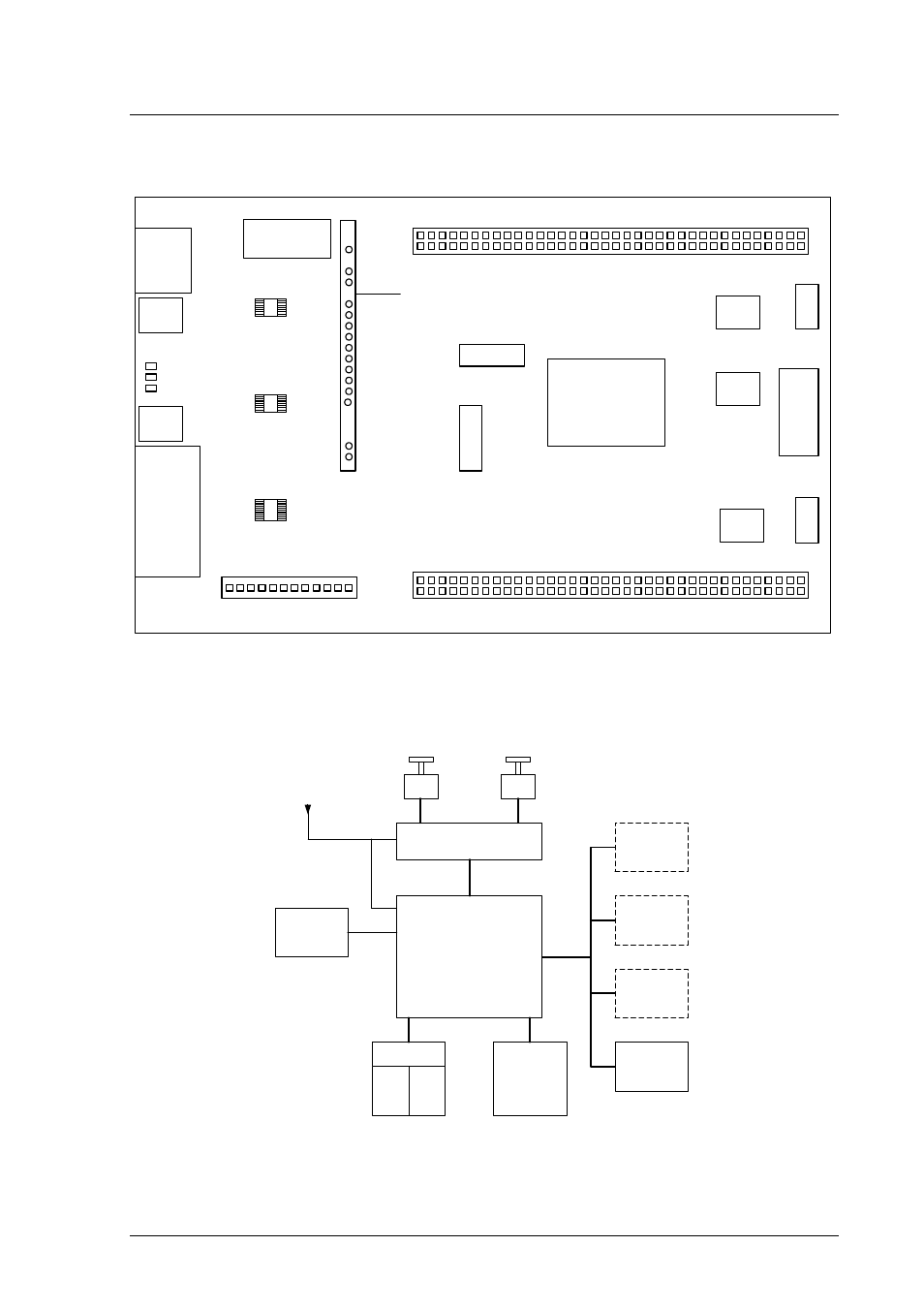
The diagram shows a general layout of the EDK board.
9-Way
D-Type
Power
RESET
Switch
NMI
Switch
User1 LED
User2 LED
Power LED
FLASH
Programming
CJ4
5V
UVcc
GND
RESn
FW
NMIn
ULED1
ULED2
PSCK
PTXD
PRXD
RX232
TX232
CTS
RTS
Microprocessor
LIN
I2C
J1
J2
XTAL
OSC
Testpoints
SPI
D
EBU
G
LIN
I2
C
F
IGURE
3-1: EDK B
OARD
L
AYOUT
3.1. EDK
B
LOCK
D
IAGRAM
The diagram shows the connectivity of the components on the EDK board.
Microprocessor
Switch De-Bounce
LIN
SPI
I2C
On-Chip
Debug
Connector
RS232
Programming
& Comms
User1
&
User2
Power
LEDs
Header
Connectors
Reset
NMI
Switches
EDK specific
External
PSU
F
IGURE
3-2: EDK B
LOCK
D
IAGRAM
5
See also other documents in the category Renesas Hardware:
- Single-Chip Microcomputer M34551T2-MCU (42 pages)
- M3T-FLX-80NRA (6 pages)
- 70 (162 pages)
- M16C/30P (102 pages)
- PROM Programming Adapter PCA7427G02 (20 pages)
- R0E572110CFK00 (40 pages)
- H8/325 Series (20 pages)
- Single-Chip Microcomputer H8/36079 (27 pages)
- Direct Dummy IC M3T-DIRECT100S (4 pages)
- M3A-2152 (95 pages)
- PCA7755D (6 pages)
- M16C/6N5 (106 pages)
- SH7085 (50 pages)
- QFP-144 (23 pages)
- H8/3834 Series (22 pages)
- RSKM16C62P (3 pages)
- H8/33937 (22 pages)
- Single-Chip Microcomputer H8SX/1622 (5 pages)
- E6000 (29 pages)
- PCA7400 (18 pages)
- PCA4738FF-64 (20 pages)
- SuperH HS7339KCU01HE (43 pages)
- M16C FAMILY (103 pages)
- PCA7412F-100 (20 pages)
- 4513 (210 pages)
- M34551E8FP (16 pages)
- Dummy IC M3T-SSOP36B-450 (4 pages)
- Emulation Pod M30100T3-RPD-E (52 pages)
- Converter Board for M30102 M30102T-PTC (4 pages)
- SH7145 (31 pages)
- HS1653ECN61H (36 pages)
- Converter Board R0E521276CFG00 (4 pages)
- PCA7302E1F-80 (18 pages)
- H8/3814 Series (21 pages)
- H8S/2646 Series (20 pages)
- SuperHTM Family SH7125 Series (40 pages)
- M30262T-PTC (4 pages)
- SH7670 (82 pages)
- H8/3864 Series (20 pages)
- Emulator System M3T-MR100 (306 pages)
- 38K0 (6 pages)
- PLQP0176KB-A (40 pages)
- Direct Dummy IC M3T-DIRECT80S (6 pages)
- PCA4738L-80A (26 pages)
- Converter Board R0E5212BACFG00 (6 pages)