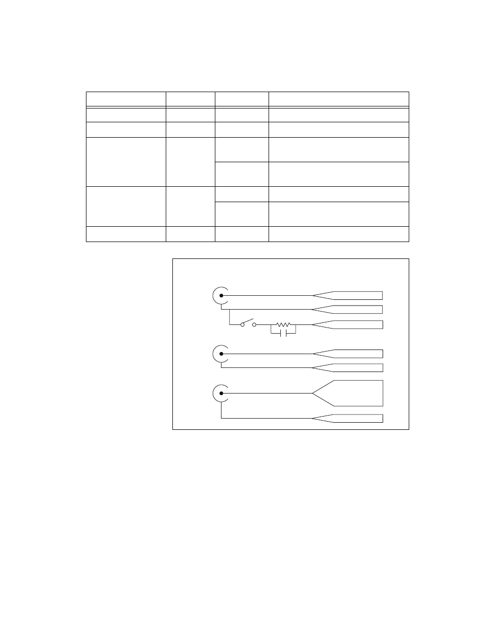
Table 1. tb-2708 signal descriptions, Figure 4. ni tb-2708 block diagram, Re 4 – National Instruments PXI Terminal Block NI TB-2708 User Manual
Page 5: E 1 for
© National Instruments Corporation
5
NI TB-2708 Installation Guide
Figure 4. NI TB-2708 Block Diagram
For more detailed descriptions of these signals, refer to the S Series User
Manual.
Additional signal configuration information is available in Measurement &
Automation Explorer (MAX). To access this information in MAX,
select your device under Devices and Interfaces, and click the Device
Routes tab.
Table 1. TB-2708 Signal Descriptions
Signal Name
Reference
Direction
Description
AI <0..3>
AI GND
Input
Analog Input channels 0 through 3.
AO <0..1>
AO GND
Output
Analog Output channels 0 and 1.
PFI 0/AI Start Trig
D GND
Input
As an input, this pin is a programmable
function input (PFI).
Output
As an output, this pin is the AI Start
Trigger signal.
PFI 7/AI SAMP CLK
D GND
Input
As an input, this pin is a PFI.
Output
As an output, this pin is the AI Sample
Clock signal.
CTR 0 OUT
D GND
Output
Counter 0 Output.
AI <0..3> +
AI <0..3> –
Front Panel
SMB Connectors
DAQ Device
Signals
AI <0..3> GND
AO <0, 1>
AO <0, 1> GND
AI Start Trig,
AI SAMP CLK,
CTR 0 OUT
D GND
5 k
Ω
0.1
μF