Philips SCC2691 User Manual
Page 16
Philips Semiconductors
Product data sheet
SCC2691
Universal asynchronous receiver/transmitter (UART)
2006 Aug 04
16
RDN
MPI
WRN
MPO
t
PS
t
PH
t
PD
SD00125
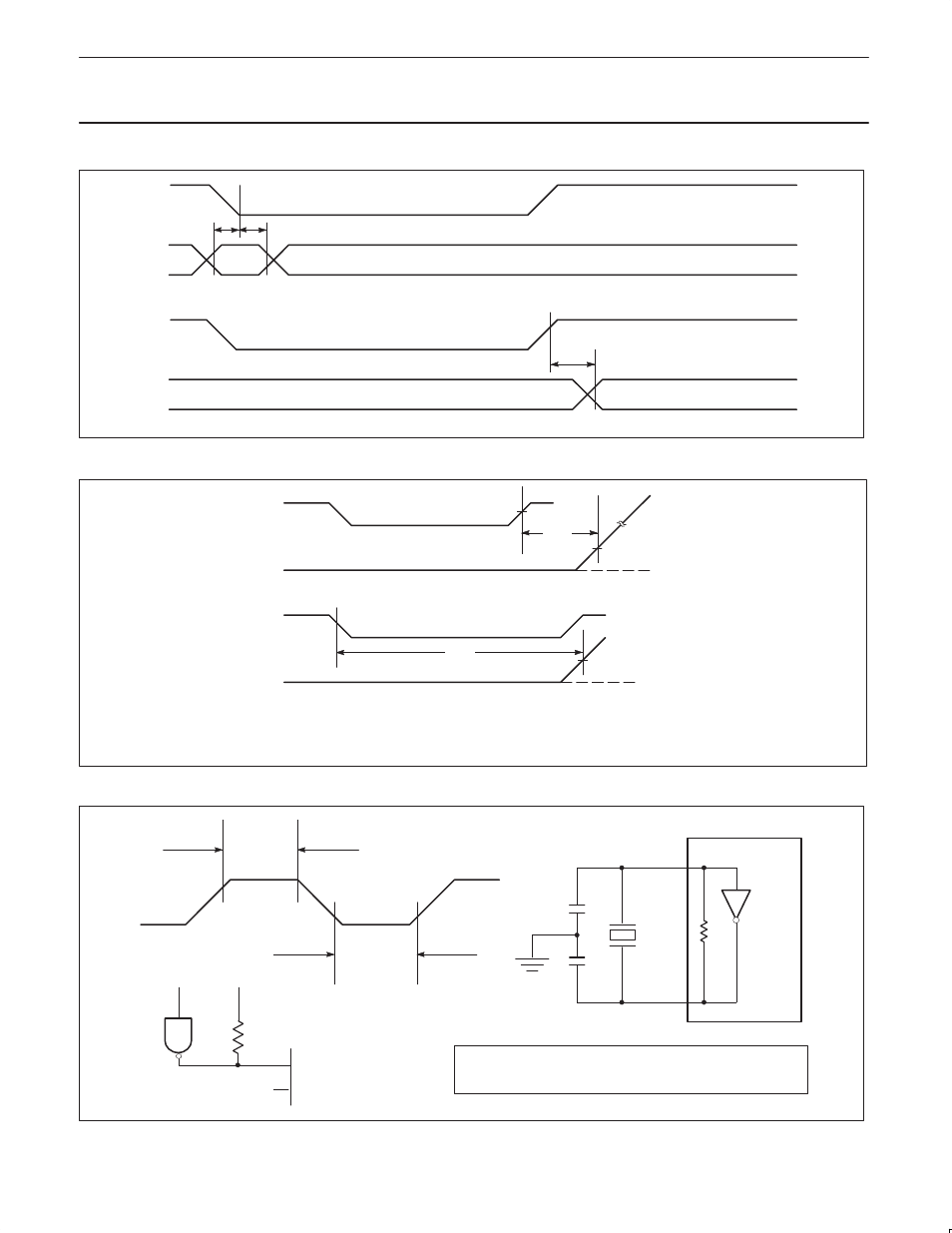
Figure 5. I/O Timing
WRN
INTERRUPT
1
OUTPUT
RDN
INTERRUPT
1
OUTPUT
V
M
t
IR
t
IR
V
OL
+0.5V
V
OL
+0.5V
V
OL
V
OL
NOTES:
1. INTRN or MPO when used as interrupt outputs.
2. The test for open drain outputs is intended to guarantee switching of the output transistor. Measurement of this response is referenced from the midpoint of the switching signal,
V
M
, to a point 0.5V above V
OL
. This point represents noise margin that assures true switching has occurred. Beyond this level, the effects of external circuitry and test environment
are pronounced and can greatly affect the resultant measurement.
SD00126
Figure 6. Interrupt Timing
X1/CLK
C/T CLK
RxC
TxC
t
CLK
t
CTC
t
Rx
t
Tx
t
CLK
t
CTC
t
Rx
t
Tx
C1
C2
Y1
X1/CLK
X2
SCC2691
Y1 = 3.6864MHz, C
L
= 20pF
C1 = C2 = 24pF
CLK
5V
470
Ω
X1
X2
N/C
TYPICAL CRYSTAL SPECIFICATION
FREQUENCY. . . . . . . . . . . . . . 2–4MHz
LOAD CAPACITANCE (C
L
). . . 20 or 32pF (typical)
TYPE OF OPERATION . . . . . .PARALLEL RESONANT, FUND. MODE
DRIVING
FROM EXTERNAL
SOURCE
50k
to
150k
SD00127
Figure 7. Clock Timing