Philips SCC2691 User Manual
Page 11
Philips Semiconductors
Product data sheet
SCC2691
Universal asynchronous receiver/transmitter (UART)
2006 Aug 04
11
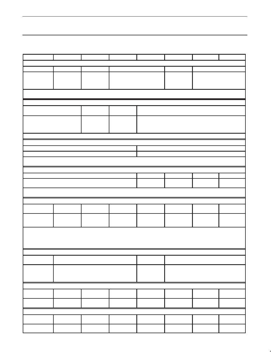
Table 2.
Register Bit Formats
Bit 7
Bit 6
Bit 5
Bit 4
Bit 3
Bit 2
Bit 1
Bit 0
MR1 (Mode Register 1)
RxRTS Control
RxINT Select
Error Mode*
Parity Mode
Parity Type
Bits per Character
0 = no
1 = yes
0 = RxRDY
1 = FFULL
0 = Char
1 = Block
00 = With parity
01 = Force parity
10 = No parity
11 = Special mode
0 = Even
1 = Odd
00 = 5
01 = 6
10 = 7
11 = 8
NOTE:
*In block error mode, block error conditions must be cleared by using the error reset command (command 4x) or a receiver reset.
MR2 (Mode Register 2)
Channel Mode
TxRTS
Control
CTS Enable
Tx
Stop Bit Length*
00 = Normal
01 = Auto echo
10 = Local loop
11 = Remote loop
0 = No
1 = Yes
0 = No
1 = Yes
0 = 0.563 4 = 0.813 8 =1.563 C = 1.813
1 = 0.625 5 = 0.875 9 = 1.625 D = 1.875
2 = 0.688 6 = 0.938 A = 1.688 E = 1.938
3 = 0.750 7 = 1.000 B = 1.750 F = 2.000
NOTE: *Add 0.5 to values shown for 0–7 if channel is programmed for 5 bits/character.
CSR (Clock Select Register)
Receiver Clock Select
Transmitter Clock Select
See Text
See Text
See Table 6 for BRG Test frequencies in this data sheet, and
“Extended baud rates for SCN2681, SCN68681, SCC2691, SCC2692, SCC68681
and SCC2698B” Philips Semiconductors ICs for Data Communications, IC-19, 1994.
CR (Command Register)
Miscellaneous Commands
Disable Tx
Enable Tx
Disable Rx
Enable Rx
See Text
0 = No
1 = Yes
0 = No
1 = Yes
0 = No
1 = Yes
0 = No
1 = Yes
NOTE:
Access to the miscellaneous commands should be separated by 3 X1 clock edges. A disabled transmitter cannot be loaded.
SR (Channel Status Register)
Received Break
Framing
Error
Parity
Error
Overrun
Error
TxEMT
TxRDY
FFULL
RxRDY
0 = No
1 = Yes
*
0 = No
1 = Yes
*
0 = No
1 = Yes
*
0 = No
1 = Yes
0 = No
1 = Yes
0 = No
1 = Yes
0 = No
1 = Yes
0 = No
1 = Yes
NOTE:
*These status bits are appended to the corresponding data character in the receive FIFO. A read of the status register provides these bits [7:5]
from the top of the FIFO together with bits [4;0]. These bits are cleared by a reset error status command. In character mode they are reset when
the corresponding data character is read from the FIFO. In block error mode, block error conditions must be cleared by using the error reset
command (command 4x) or a receiver reset.
ACR (Auxiliary Control Register)
BRG Set
Select
Counter/Timer
Mode and Source
Power-Down
Mode
MPO Pin
Function Select
0 = Set 1
1 = Set 2
See Text
0 = On
PWRDN Active
1 = Off
Normal
000 = RTSN 100 = RxC (1X)
001 = C/TO 101 = RxC (16X)
010 = TxC (1X) 110 = TxRDY
011 = TxC (16X) 111 = RxRDY/FFULL
ISR (Interrupt Status Register)
MPI Pin
Change
MPI Pin
Current State
Not used
Counter
Ready
Delta
Break
RxRDY/
FFULL
TxEMT
TxRDY
0 = No
1 = Yes
0 = Low
1 = High
0 = No
1 = Yes
0 = No
1 = Yes
0 = No
1 = Yes
0 = No
1 = Yes
0 = No
1 = Yes
IMR (Interrupt Mask Resister)
MPI Change
Interrupt
MPI Level
Interrupt
Not used
Counter
Ready Int
Delta Break
Interrupt
RxRDY/FFULL
Interrupt
TxEMT
Interrupt
TxRDY
Interrupt
0 = Off
1 = On
0 = Off
1 = On
0 = Off
1 = On
0 = Off
1 = On
0 = Off
1 = On
0 = Off
1 = On
0 = Off
1 = On