4 block diagram – Premio Computer Apollo/Shadowhawk User Manual
Page 39
Intel Desktop Board D845HV/D845WN Technical Product Specification
16
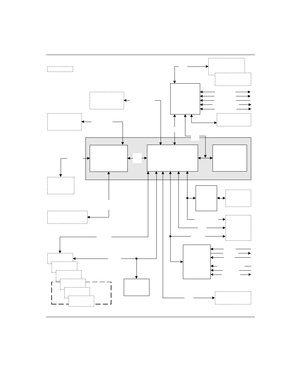
1.2.4
Block Diagram
Figure 3 is a block diagram of the major functional areas of the D845HV and D845WN boards.
D845WN
Only
845 Chipset
82801BA
I/O Controller Hub
(ICH2)
82845 Memory
Controller Hub
(MCH)
82802AB 4 Mbit
Firmware Hub
(FWH)
AHA
Bus
System Bus
(400 MHz)
mPGA478
Processor Socket
Primary/
Secondary IDE
Diskette Drive
Connector
LPC I/O
Controller
PS/2 Keyboard
PS/2 Mouse
Parallel Port
Serial Ports
UDMA 33 and
ATA-66/100
USB
LPC
Bus
Hardware
Monitor
(optional)
OM12274
Back Panel
USB Ports (2)
AD1885
Audio Codec
(optional)
Auxiliary Line In
Mic In
Line Out
CD-ROM
Line In
CNR
Connector
(optional)
LAN
Connector
(optional)
Physical
Layer
Interface
(optional)
PCI Slot 1
PCI Slot 2
PCI Slot 3
PCI Slot 4
PCI Slot 5
CSMA/CD
Unit Interface
DIMM Banks (3)
AGP
Interface
4X AGP
Connector
(1.5 V only)
= connector or socket
Telephony
PCI Bus
PCI Slot 6
SMBus
AC Link
USB
SDRAM
Bus
Back Panel
USB Ports (2)
Front Panel
USB Ports (2)
USB
USB
Infrared Port
Figure 3. Block Diagram