Frequency synthesizer unit, Control circuit, Tk-8180 – Kenwood TK-8180 User Manual
Page 18: Circuit description

TK-8180
18
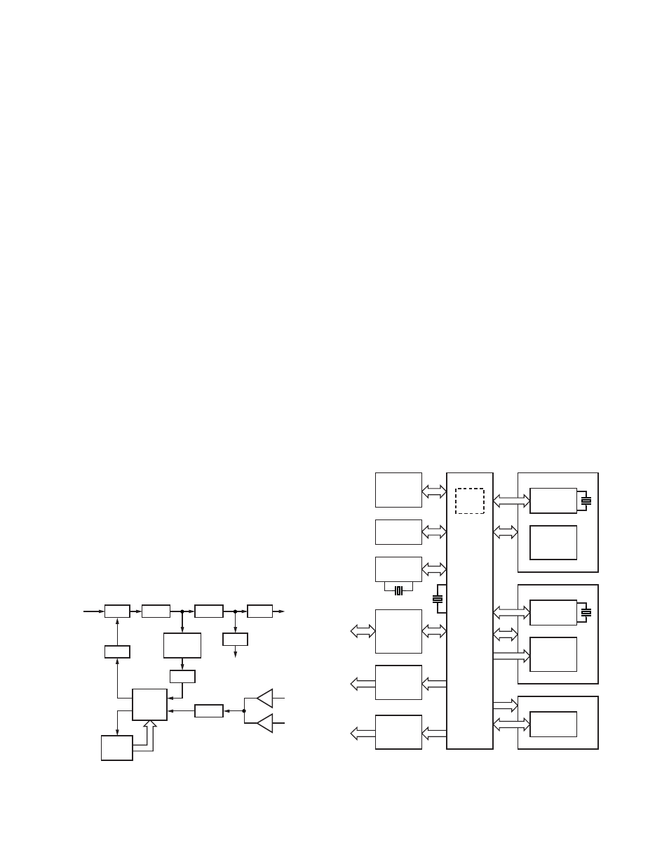
4. Frequency Synthesizer Unit
4-1. Frequency Synthesizer
The frequency synthesizer consists of the TCXO (X301),
VCO, PLL IC (IC301) and buffer amplifiers.
The TCXO generates 16.8MHz. The frequency stability is
2.5ppm within the temperature range of –30 to +60
°C. The
frequency tuning and modulation of the TCXO are done to
apply a voltage to pin 1 of the TCXO. The output of the TCXO
is applied to pin 8 of the PLL IC.
The VCO consists of 2VCO and covers a dual range of the
405.15~475.15MHz and the 450~520MHz. The VCO gener-
ates 405.15~475.15MHz for providing to the first local signal
in receive. The operating frequency is generated by Q307 in
transmit mode and Q306 in receive mode. The oscillator fre-
quency is controlled by applying the VCO control voltage, ob-
tained from the phase comparator (IC301) to the variable ca-
pacitor diodes (D308 and D311 in transmit mode and D309
and D313 in receive mode).
The T/R pin of IC404 goes “high” in receive mode causing
Q307 and Q309 to turn off, and Q306, Q308 and Q310 turn
on. The T/R pin goes “low” in transmit mode.
The outputs from Q306 and Q307 are amplified by buffer
amplifier (Q311) and doubled by Q301 and then sent to PLL
IC.
The PLL IC consists of a prescaler, reference divider,
phase comparator, charge pump (The frequency step of the
PLL circuit is 20 or 25kHz). The input signal from the pins 8
and 5 of the PLL IC is divided down to the 20 or 25kHz and
compared at phase comparator. The phase comparator out-
put signal is fed into a low-pass filter (Q302 and Q303) before
being applied to the VCO as a frequency control voltage. This
low-pass filter’s power is supplied by the DC/DC converter
(IC251 and Q251). The DC signal is applied to the CV of the
VCO and locked to keep the VCO frequency constant.
PLL data is output from DT (pin 112), PCK (pin 82) and PLE
(pin 81) of the microprocessor (IC404). The data are input to
the PLL IC when the channel is changed or when transmis-
sion is changed to reception and vice versa. A PLL lock con-
dition is always monitored by the pin 80 (UL) of the micropro-
cessor. When the PLL is unlocked, the UL goes low.
5. Control Circuit
The block diagram of the control circuit is shown in Figure
5.
The CPU (IC404) is a 16-bit microcomputer that contains a
256k-byte Mask ROM and a 20k-byte RAM. This CPU is con-
nected with an external 512k-byte Flash ROM (IC405) and
operates in memory expansion mode.
The Firmware Program is stored in the Flash ROM and the
user data and adjustment data are stored in the EEPROM
(IC401). The CPU and Flash ROM are connected with an 8 bit
bus and the EEPROM and RTC IC (IC402) are connected with
a I2C bus (*1). The RTC IC (IC402) has a clock function and is
controlled by the CPU (IC404).
Serial communication with a PC is performed through two
paths: through the 232C Level converter IC (IC416) and
through the Display Unit Panel CPU (IC902). The 8 bit Shift
Register (IC403) is used as an 8-port Extended Output Port.
IC410 is an 8 bit-8ch D/A converter. The channels are set as
follows:
Ch1 : Modulation balance
Ch2 : Deviation Factor
Ch3 : Max Power Level
Ch4 : Reception tuning circuit
Ch5 : Deviation Factor
Ch6 : Speaker volume
Ch7 : VCXO control voltage
Ch8 : DEO output level
*1: I2C bus is a registered trademark of PHILIPS of the Neth-
erlands.
LPF
BPF
BUFF
VCO
PLL
CPU
20
15
5
Doubler
x2
CV
Q313
BUFF
Q311
TCXO
X301
SW
D316
SW D315
To
drive
amp
Q301
To mixer
8
FC
BAL
IC408
MB
T/R
T/R
(TX : Low)
IC301
UL
IC404
DT,PCK,PLE
Q302
Q303
CIRCUIT DESCRIPTION
Fig. 4
PLL block diagram
IC405
Flash
ROM
IC403
8bit Shift
register
IC410
D/A
converter
IC416
232C
Level
converter
IC902
CPU
IC903
LCD
driver
IC401
EEPROM
IC402
RTC IC
Display unit
IC415
AQUA-L
IC413
Multi-
plexer
Signal block
IC301
PLL IC
RF block
Mask
ROM
IC404
CPU
Fig. 5
Control circuit block diagram
