Sony Ericsson GR64 User Manual
Page 35
LZT 123 1834
35
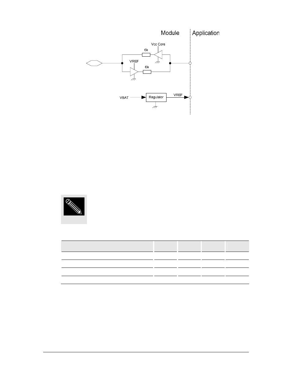
Figure 5.3-1 Common Level Shifter Circuit (VREF as an Output)
The output impedance of the Maxim chip is 6kohm, so you must ensure that your
application impedance to ground or supply is high enough to allow for full voltage
swing. A minimum application impedance of 56kohm should be assumed. Similarly,
where a GPIO is used as an input, your application driver output impedance must not
exceed 680 ohm.
The GR64 VREF can be configured as an output (to the host application) or an input
(from the host application), as defined in section 5.6.
Any GPIO that is used truly bi-directional cannot be open drain type on
both sides. At least one side needs to be able to drive the signal both
high and low.
Table 5.3-1 Level shifter IO logic levels
Parameter
Min
Nom
Max
Unit
IO input voltage high threshold (V
IHC
)
VREF-0.4
V
IO input voltage low threshold (V
ILC
) 0.4
V
IO output voltage high threshold (V
OHC
)
VREF-0.4
V
IO output voltage low threshold (V
OLC
) 0.4 V
The level shifter IO interfaces have typical input and output rise/fall times of 25ns.
NOTE