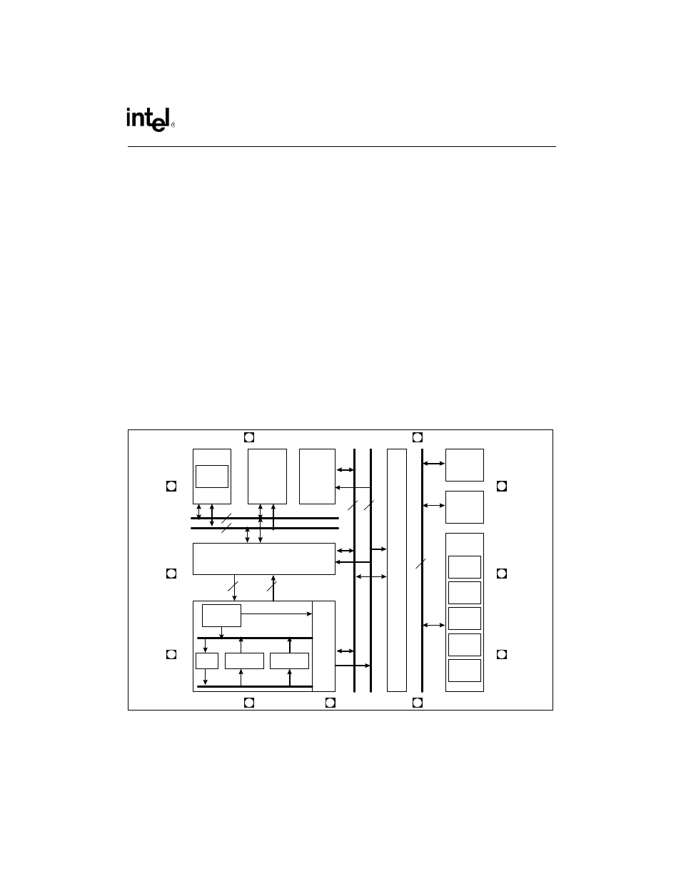
0 introduction to the 8xc251tx, 1 comparing the 8xc251tx and 8xc251sx, Figure 1. 8xc251tx block diagram – Intel 8xC251TB User Manual
Page 7: 8xc251tx hardware description

1
8xC251Tx Hardware Description
1.0 INTRODUCTION TO THE 8xC251Tx
This Hardware Description describes the 8xC251TB, 8xC251TQ (referred to collectively as the 8xC251Tx)
embedded microcontroller, which is the newest member of the MCS
®
251 microcontroller family. The
8xC251Tx is pin and code compatible with the 8xC251Sx but is enhanced with the addition of new features.
This document addresses the differences between the two members of the MCS 251 microcontroller family.
For a detailed description of the MCS 251 microcontroller core and standard peripherals shared by both the
8xC251Sx and 8xC251Tx, please refer to the 8xC251SA, 8xC251SB, 8xC251SP, 8xC251SQ Embedded
Microcontroller User’s Manual (272795).
1.1
Comparing the 8xC251Tx and 8xC251Sx
The differences between the 8xC251Tx and the 8xC251Sx are briefly described here.
•
The maximum operating frequency of the 8xC251Tx is 24 Mhz compared to 16 MHz for the 8xC251Sx.
•
The 8xC251Tx has two serial I/O ports while the 8xC251Sx has one. The pins for the second serial I/O
port are multiplexed with other functional pins.
•
The 8xC251Tx has a new configuration option (Extended Data Float timing) to allow interfacing with
slower memories. This feature is supported by a bit in the configuration byte, UCONFIG1. The corre-
sponding bit in the 8xC251Sx has a different function.
•
The 8xC251Tx is offered in with factory programmed ROM while the 8xC251Sx is also offered with
OTPROM/EPROM.
Figure 1. 8xC251Tx Block Diagram
PORT
0-3
EPROM/
ROM
RAM
BUS INTERFACE UNIT
Instruction
Sequencer
ALU
Register
File
Program
Counter
Clock and
Reset Unit
Interrupt
Handler Unit
Peripherals
3 Timers
WDT
PCA
Serial I/O
8
24
8
16
INSTR
24
PC
16
16
Memory Data
Memory Address
Da
ta B
u
s
Da
ta
Ad
d
res
s
IB
B
u
s
P
eri
p
h
er
al
In
te
rfa
ce
U
n
it
D
at
a M
emo
ry
In
te
rfa
ce
CPU
SRC1, SRC2
DST
RESET
P0 (A7-
0/D7-0)
P2 (A15-8)
P3
PSEN
ALE
VCC
VSS
P1
XTAL1
XTAL2
2nd Serial
I/O
