Connector j2 interconnect signals (mvme712-13, mvm, Table 3-5. connector j2 interconnect signals (mvme, Connector j3 interconnect signals (lcp2 adapter) c – Motorola MVME712B User Manual
Page 42: Table 3-6. connector j3 interconnect signals (lcp2, Table 3-5, Table 3-6
Interconnect Signals
MVME712A/D3
3-9
3
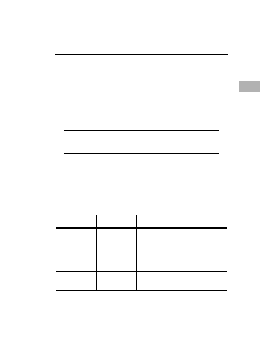
Connector J2 Interconnect Signals (MVME712-13, MVME712AM)
Connector J2 is a backplane modem power connector. Each pin connection,
signal mnemonic, and signal characteristic for the connector is listed in
.
Connector J3 Interconnect Signals (LCP2 Adapter) Connector:
Connector J3 on the LCP2 adapter is the SCSI port. Each pin connection, signal
mnemonic, and signal characteristic for the connectors is listed in
.
Table 3-5. Connector J2 Interconnect Signals (MVME712-13/AM)
Pin
Number
Signal
Mnemonic
Signal Name and Description
1
+5VMODEM
+5 Vdc Power - supplied by the backplane and
routed to J20.
2
+12VMODEM
+12 Vdc Power - supplied by the backplane and
routed to J20.
3
-12VMODEM
-12 Vdc Power - supplied by the backplane and
routed to J20.
4
GND
GROUND
5,6
Not used.
Table 3-6. Connector J3 Interconnect Signals (LCP2 Adapter)
Pin
Number
Signal
Mnemonic
Signal Name and Description
1
GND
GROUND
2
DB00*
DATA bus (bit 0) - least signiÞcant bit and the
lowest priority during the arbitration phase.
3
GND
GROUND
4
DB01*
DATA bus (bit 1)
5
GND
GROUND
6
DB02*
DATA bus (bit 2)
7
GND
GROUND
8
DB03*
DATA bus (bit 3)
9
GND
GROUND