Finisar AN-2030 User Manual
Page 34
AN-2030: Digital Diagnostic Monitoring Interface for Optical Transceivers
F i n i s a r
9/26/02 Revision D
Page 34
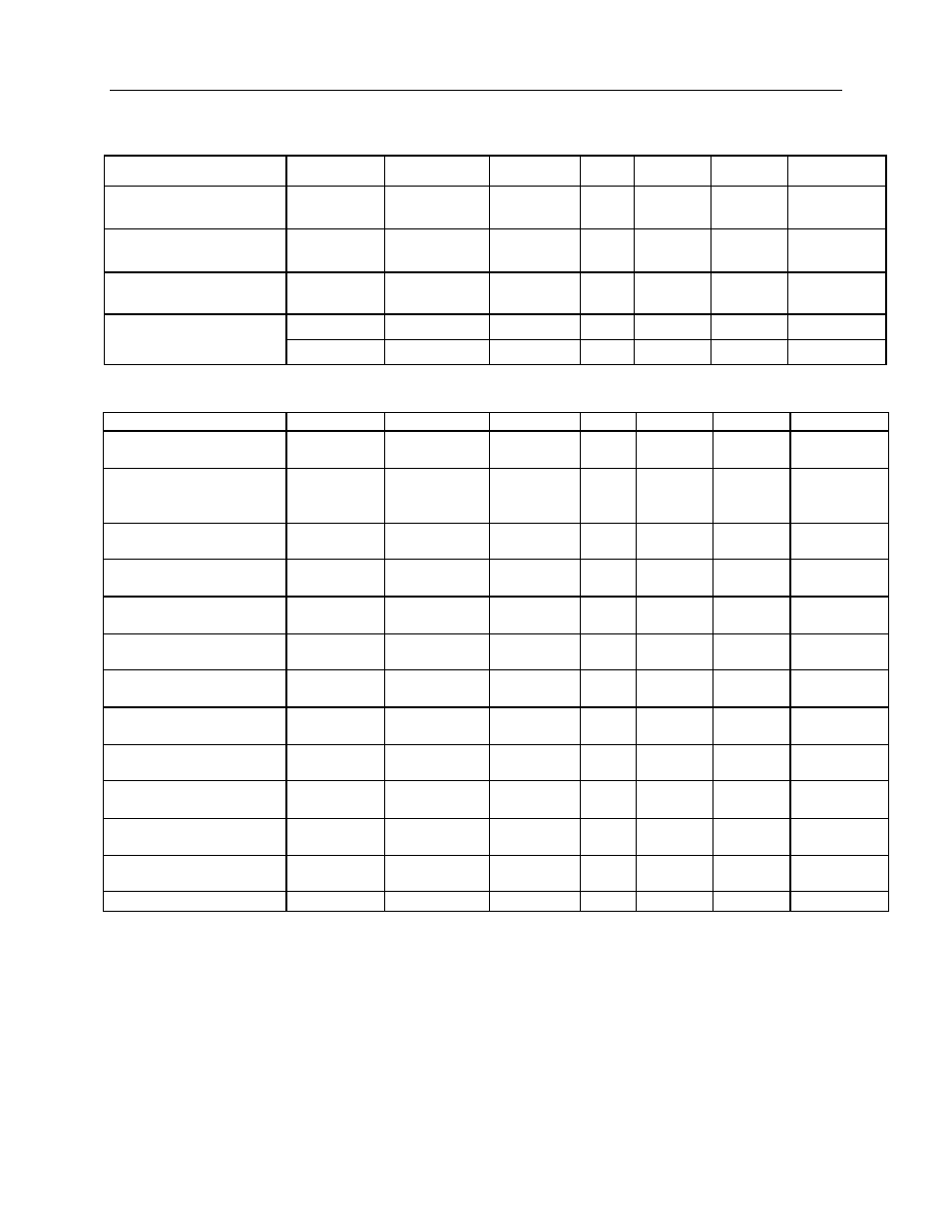
DC ELECTRICAL CHARACTERISTICS
( Vcc = 3.15V to 3.60V)
PARAMETER
SYMBOL
CONDITION
MIN
TYP
MAX
UNITS
NOTES
Input Leakage (SDA,
SCL)
I
LI
-1
+1
µ
A
2
Input Logic 1 (SDA,
SCL)
V
IH
0.7Vcc
Vcc+0.5
V
1
Input Logic 0 (SDA,
SCL)
V
IL
GND-0.5
0.3Vcc
V
1
I
OL1
0.4V
3
mA
1
Low Level Output
Current (SDA)
I
OL2
0.6V
6
mA
1
AC ELECTRICAL CHARACTERISTICS
( Vcc = 3.15V to 3.60V)
PARAMETER
SYMBOL
CONDITION
MIN
TYP
MAX
UNITS
NOTES
SCL clock frequency
fSCL
0
0
400
100
kHz
*,3
**
Bus free time between
STOP and START
condition
tBUF
1.3
4.7
µ
s
*,3
**
Hold time (repeated)
START condition
tHD:STA
0.6
4.0
µ
s
*,3,4
**
Low period of SCL
clock
tLOW
1.3
4.7
µ
s
*,3
**
High period of SCL
clock
tHIGH
0.6
4.0
µ
s
*,3
**
Data hold time
tHD:DAT
0
0
0.9
µ
s
*,3,5,6
**
Data set-up time
tSU:DAT
100
250
ns
*,3
**
Start set-up time
tSU:STA
0.6
4.7
µ
s
*,3
**
Rise time of both SDA
and SCL signals
tR
20+0.1CB
300
1000
ns
*
**
Fall time of both SDA
and SCL signals
tF
20+0.1CB
300
300
ns
*
**
Set-up time for STOP
condition
tSU:STO
0.6
4.0
µ
s
*
**
Capacitive load for
each bus line
CB
400
pF
EEPROM write time
T
W
10
ms
* Fast mode
** Standard mode
Notes
1. All voltages are referenced to ground.
2. Input levels equal either Vcc or GND.
3. The output must be configured to source.
4. The output must be configured to have pull-up resistance enabled.
5. This is the time for one comparison. The cycle is multiplied by 3.
6. This parameter is measured with maximum output current.