Block diagram, Handling the board, Block diagram –2 – Altera Santa Cruz User Manual
Page 6: Handling the board –2
1–2
Chapter 1: Overview
Handling the Board
Santa Cruz, USB, MICTOR, SD Card HSMC Reference Manual
© December 2008 Altera Corporation
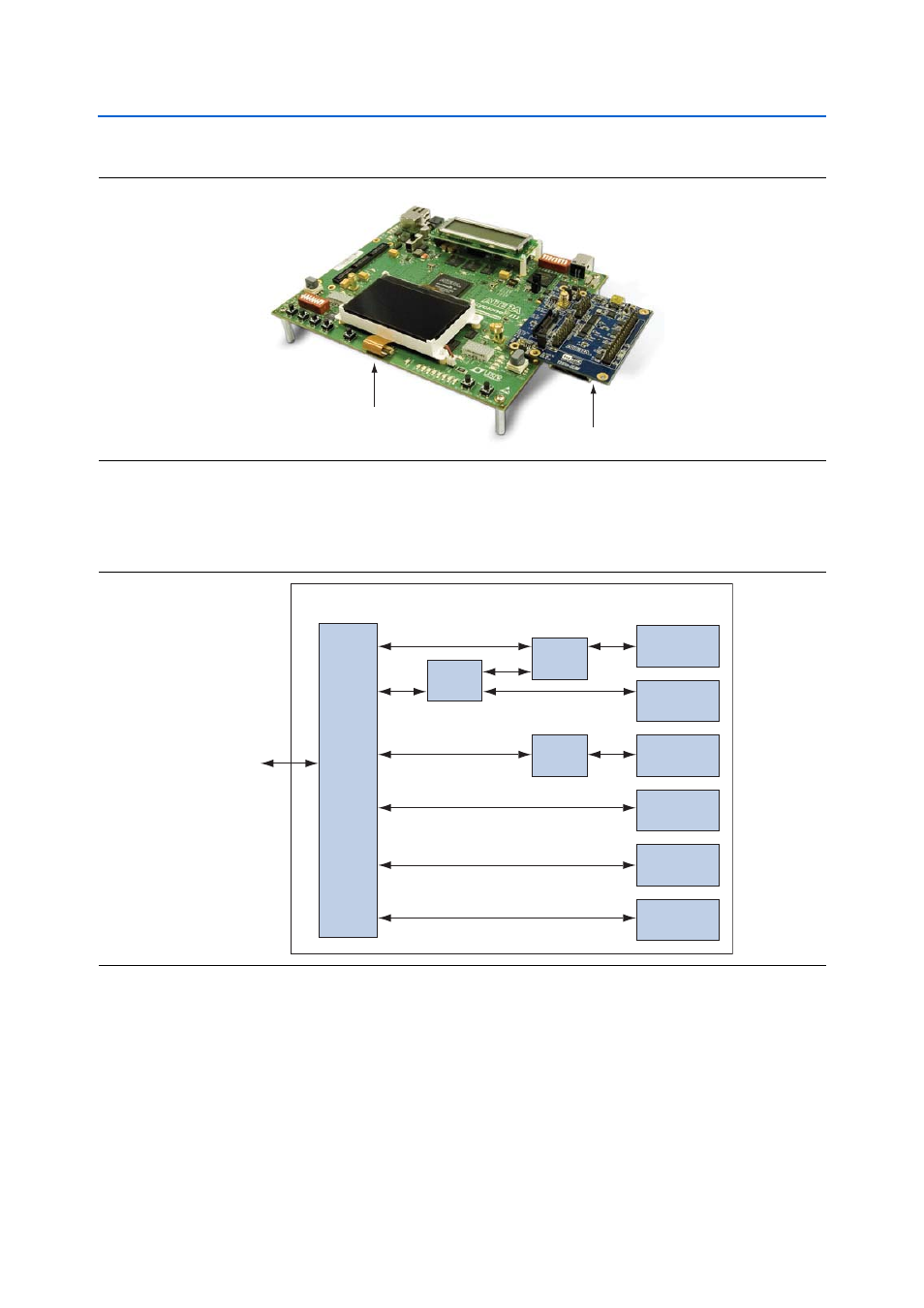
Block Diagram
shows the functional block diagram of the THDB-SUM board.
Handling the Board
When handling the board, it is important to observe the following precaution:
c
Static Discharge Precaution: Without proper anti-static handling, the board can be
damaged. Therefore, use anti-static handling precautions when touching the board.
Figure 1–1. THDB-SUM Board Connected to the Cyclone III FPGA Development Board
THDB-SUM Board
Cyclone III FPGA Development Board
Figure 1–2. THDB-SUM Board Block Diagram
HSMC
Connector
Santa Cruz
Connector
USB
Transceiver
SD Card
Socket
MICTOR
Connector
SMA
Connector
Level
Shifters
Level
Shifters
Bus Switch
SC
Interface
USB Interface
SD Card Interface
MICTOR Connector Interface
External Clock Input
THDB-SUM
To
HSMC Interface
Host Board
Interface
2
I C
Serial
EEPROM
2
I C