Hitachi HUS103036FL3800 User Manual
Page 37
Drawing No. Sheet No. Revision
K6610091
37/43 2005/2/23
11.2 Other connectors
Table 11.5 Pin assignment of Auxiliary Connector C4
(WIDE LVD drive)
Pin
No. Signal
Name Pin
No.
Signal
Name
Note
1 -ID0 2
Reserved
3 -ID1 4
Reserved
5 -ID2 6
Reserved
7
-ID3
8
LED(with 150 ohm)
See Figure 12.1
9 N.C. 10 GND
11 5V 12
-WRITE
PROTECT
Table 11.6 Pin assignment of Option Jumper Connector C3
(WIDE LVD drive)
Pin No.
Signal Name
Pin No.
Signal Name
Note
1 -ID3 2 GND
3 -ID2 4 GND
5 -ID1 6 GND
7 -ID0 8 GND
9
-Disable Auto Start
10
GND
11 -Force
Single-Ended
mode 12
GND
13
-Enable Delayed Start
14
GND
15 -Write
Protect 16
GND
17 Reserved 18 GND
19 Reserved 20 GND
21
LED(with 0 ohm)
22
5V(with 150 ohm)
See Figure 12.1
23
Term. Power to SCSI bus
24
Term. Power to SCSI bus
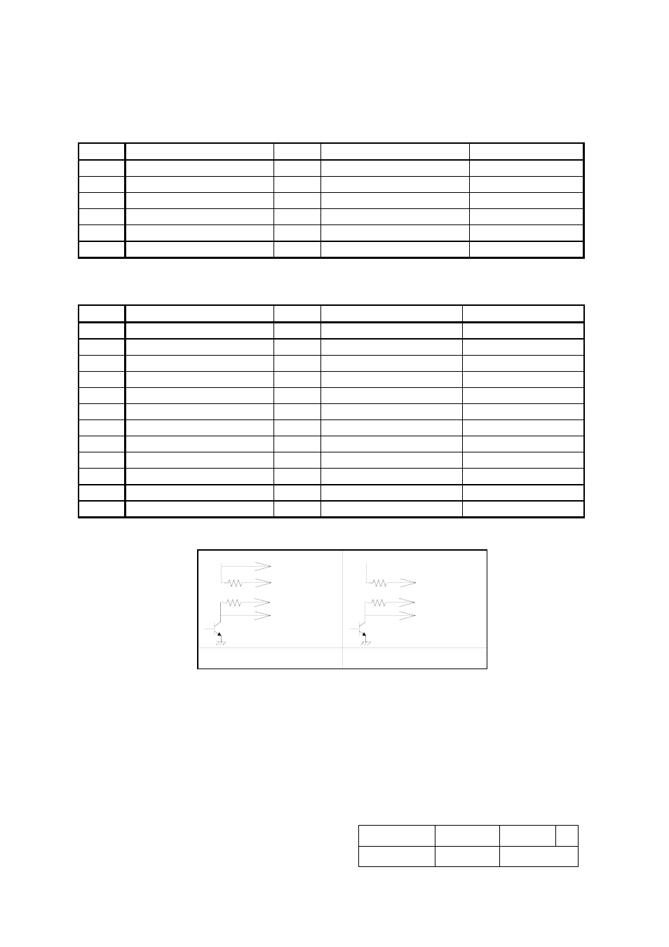
LED (C3-21)
150 ohm
+5V
5V (C3-22)
NW drive
5V (C4-11)
LED (C4-8)
150 ohm
LED (C3-21)
150 ohm
+5V
5V (C3-22)
NC drive
LED (C1-77)
0 ohm
Figure 11.1 LED Driver