4 notice at data input – Hitachi SJ-DG User Manual
Page 19

CHAPTER 5 FUNCTION
13
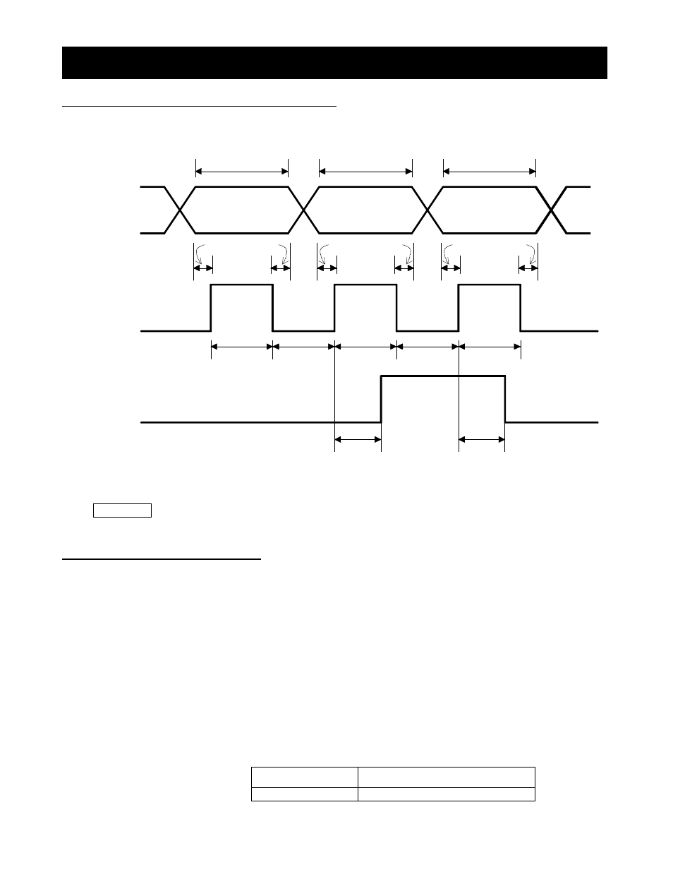
5.3.2 TIMING AT TWO DIVIDING DATA INPUT
Take in data in on-edge of strove signal. Let on/off time of strobe signal be more than 20ms. And let off time of
strobe signal be more than 20ms,
Precaution If Figure 5.3.2 timing chart is not satisfied, be careful because of possibility of taking in error
data.
5.4 NOTICE AT DATA INPUT
While inputting the data by terminal of SJ-DG, notice the following items.
(1) Each input is possible to set within data range of the inverter in every setting item. If inputting without data
range, sequence error is outputted and data input is invalid (previous data is kept).
(2) If classification code is inputted in dividing input mode, make sure to input classification code in order, higher
code, and then lower code. If lower code is inputted at first, sequence error is outputted and data input is
invalid (previous data is kept)
(3) Re-input of correct data, or reset of inverter, or power off carries out cancellation of sequence error. And, if
two times input are correct in dividing input mode, they are cancelled just after second input.
(4) If a code without codes in table of classification is inputted, sequence error is outputted.
(5) In case of trip of inverter, data input is invalid. Make sure to reset inverter and re-input.
(6) When each command destination of inverter is not set to option board put on, do not input data.
(7) If setting frequency is input in “rate”, do the following process below.
(Example) If 75% of max frequency is set, input
in
I
is
M
I
in
×
=
75
.
0
75
.
0
rate
M
input data full scale
Switch type 1
Input data full scale value(
M
)
BIN
65535
ON
OFF
OFF
OFF
OFF
OFF
OFF
ON
ON
ON
Dn
(n=0-15)
STRB
Within 20ms
Within 20ms
At load current 20mA
SEQ
(Sequence error output)
More than
20ms
More than
20ms
More than
20ms
More than
20ms
More than
20ms
Data definite
period
Data definite
period
Data definite
period
Normal data
Abnormal data
Normal data
More than 0ms
More than 0ms
More than 0ms
Figure 5.3.2 Timing chart of two dividing data input
