Avago Technologies ACPL-H342-000E User Manual
Page 3
For product information and a complete list of distributors, please go to our web site:
www.avagotech.com
Avago, Avago Technologies, and the A logo are trademarks of Avago Technologies in the United States and other countries.
Data subject to change. Copyright © 2005-2010 Avago Technologies. All rights reserved.
AV02-2653EN - September 24, 2010
Test Connection and Operation
The denotations or symbols used below refer to High Side, the top gate driver (U1) operation. If operating in a half-
bridge topology, please refer to the bottom gate driver’s (U2) denotations or symbols in schematic diagram, Figure 2.
ACPL-H342/K342 Input Side:
1.
LED input current:
ACPL-H342/K342 has a LED input gate control. Split resistors network R1 and R2, each with a value of
170
: are used to achieve high CMR response. Connecting “TP_ANODE_T” and “TP_CATHODE_T” to a 5 V input pulse
signal will drive a recommended LED current of 10 mA.
ACPLH342/K342 Output Side:
1.
Output positive power supply:
Connect the +15 V of an isolated DC power supply to “VCC_T” and the common to “TP_
E1_T” test points. “TP_E1_T” is connected to the IGBT emitter.
2.
Output negative power supply (optional):
If only single positive output power supply is required, short the open
connection J4. For negative output power supply, connect the -15 V of the isolated DC power supply to “TP_VEE_T”
and the common to “TP_E1_T” test points. Remove any short circuit connection on J4 and replace J4 with appropriate
bypass capacitors.
3.
Output positive bootstrap power supply (optional for Top, High side only):
For single positive output power supply, short
the open connection J4. Connect the +15 V power supply of the Bottom side, “VCC_B” to the Top side “VCC_T”. To
complete the bootstrap power supply, solder appropriate bootstrap resistor “Rbs”, diode “Dbs” and Capacitor “Cbs”.
4.
Gate resistors:
Solder appropriate R3 for IGBT gate discharging and R4 for IGBT gate charging.
5.
Active Miller Clamp:
If Miller clamp feature is required. Short the open connection J5. If Miller clamp feature is not
required, remove any short circuit connection on J5. It is also recommended to connect the floating Miller clamp pin
to VEE by shorting “TP_CLAMP_T” to “ TP_VEE_T” when not in used.
6.
Output:
Monitor the output or the gate of IGBT by connecting an oscilloscope between “TP_OUT_T” to “TP_E1_T”.
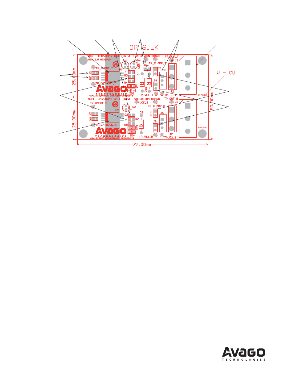
PCB Mounting
Terminal Blocks
J3 and J8
IGBT TO-220/247
type package
ACPL-H342/K342
Top Gate Driver
Bootstrap Capacitor,
Resistor and Diode
Bypass Cap
C1 and C2
Isolation
Barrier
Split Resistors
Input LED Driver
Gate Resistors
R3, R4, R7 and R8
ACPL-H342/K342
Bottom Gate Driver
Active Miller Clamp
Jumpers J5 and J10
Negative Power Supply
Jumpers J4 and J9
Figure 3. Top Layer View