Avago Technologies ACPL-H342-000E User Manual
Page 2
2
TP_ANODE_T
12
TP_CATHODE_T
Anode
1
NC
2
Cathode
3
NC
4
VEE
5
Vclamp
6
Vout
7
Vcc
8
U1
ACPL-H342/K342
11
2
170
:
R1
1
170
:
R2
1
2
1
PF
50 V
C1
1
2
NM
EC1
1
2
NM
Cbs
1
21
NM
R3
1
2
NM
R4
2
SS32
D1
1
2
NM
Dbs
1
2
NM
Rbs
1
VCC_T
1
ZD1
1
22
ZD2
1
2
2P_HEADER
1
TP_CLAMP_T
1
TP_OUT_T
1
2
J4
2P_HEADER
1
TP_VEE_T
1
TP_E1_T
1
2
3
NM
J1
3P_TO220
1
2
3
NM
J2
3P_TO247
1
2
3
NM
J3
3P_HEADER
G1
C1
E1
TP_G1
TP_C1
TP_E1
J5
Anode
NC
Cathode
NC
VEE
Vclamp
Vout
Vcc
1
2
1
PF
50 V
C2
1
2
TP_ANODE_B
12
TP_CATHODE_B
1
2
3
4
5
6
7
8
U2
ACPL-H342/K342
11
2
170
:
R5
1
170
:
R6
NM
EC2
1
21
NM
R7
1
2
NM
R8
2
SS32
D2
1
VCC_B
1
ZD3
1
22
ZD4
1
2
J10
2P_HEADER
1
TP_CLAMP_B
1
TP_OUT_B
1
2
J9
2P_HEADER
1
TP_VEE_B
1
TP_E2_B
1
2
3
NM
J6
3P_TO220
1
2
3
NM
J7
3P_TO247
1
2
3
NM
J8
3P_HEADER
G2
C2
E2
TP_G2
TP_C2
TP_E2
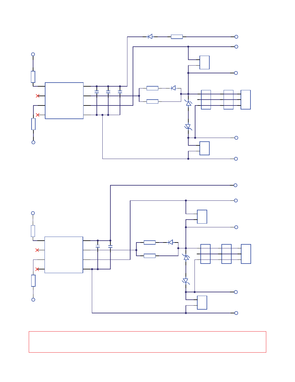
Figure 1. Schematic Diagram for ACPL-H342/K342 Evaluation Board – Top
Figure 2. Schematic Diagram for ACPL-H342/K342 Evaluation Board – Bottom
CAUTION: When operating the board connected to a half-bridge dual IGBT (with the dual IGBT connected to high-voltage
rails) never short the output ground planes and scope ground together!! Also when probing points on the upper gate-drive
channel use a scope with adequate voltage rating!