Avago Technologies MGA-81563 User Manual
Page 2

Page 2 of 6
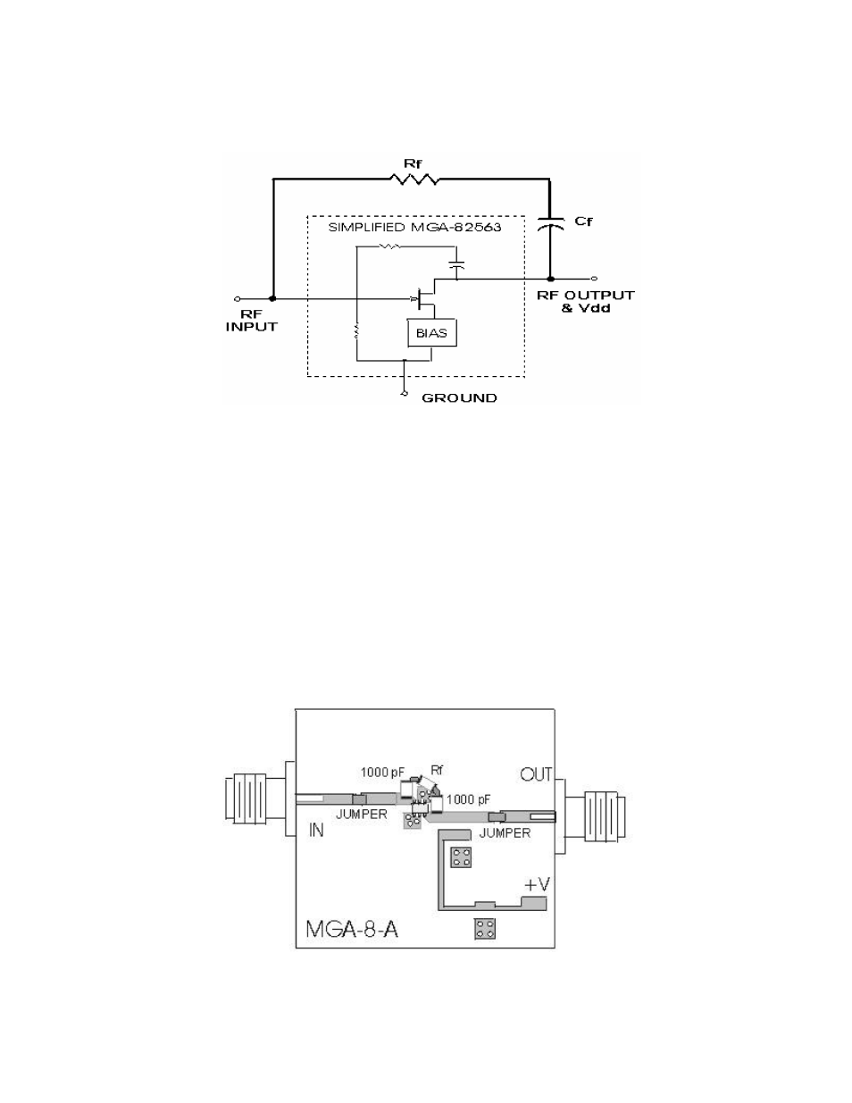
By adding a series R-C from the RF output to the RF input of the MGA
amplifier, the low-end frequency response becomes limited only by the
value of the DC blocking capacitor used in the external RF feedback loop.
Figure 1. MGA-82563 Schematic with External Feedback.
A circuit based on the MGA-8-A evaluation PCB was assembled with an
MGA-82563 to test the external feedback method. The DC blocking
capacitors normally used at both the input and output were replaced with
jumpers and the device was biased externally.
The assembled test circuit is shown in Figure 2. The external feedback
resistor, Rf, is mounted in between two 1000 pF chip capacitors on either
side of the amplifier package. Capacitor Cf was implemented with two
capacitors instead of one to simplify physically bridging around the MGA-
82563.
Figure 2. Test Circuit with External Feedback Circuit.
Test results for the external feedback circuit are shown in Figure 3. This plot
shows both gain and input return loss from 300 kHz to 1 GHz with several
