Selection guide, Pin assignment – Epson S1F77B01 User Manual
Page 7
6. SELECTION GUIDE
S1F77B01 Technical Manual (Rev.1.3)
EPSON
3
6. SELECTION GUIDE
S1F77B01 * * * * 0 * *
a b c d e
a Package
type
SOT23 5PIN “Y”
WCSP 4PIN “B”
b
Indicates a value that is ten times the detecting voltage.
c
For CMOS output, delay 50ms
“C”
For CMOS output, delay 100ms
“D”
For CMOS output, delay 200ms
“E”
For Nch open drain output, delay 50ms
“L”
For Nch open drain output, delay 100ms
“M”
For Nch open drain output, delay 200ms
“N”
d
Fixed to 0 in this IC.
e Taping
form
TR type “0R”
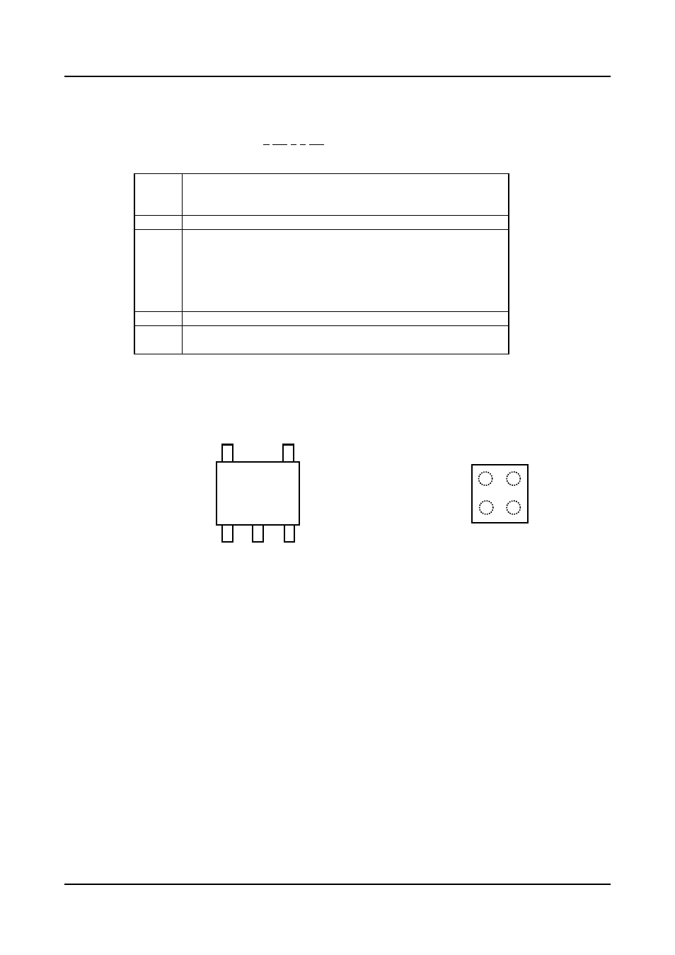
7. PIN ASSIGNMENT
DS
1 3
5
V
SS
V
DD
V
OUT
4
2
NC
DS
1 2
3
V
SS
V
DD
4
V
OUT
SOT23 5PIN
WCSP 4PIN
Top View