Block diagram – Epson S1F77B01 User Manual
Page 6
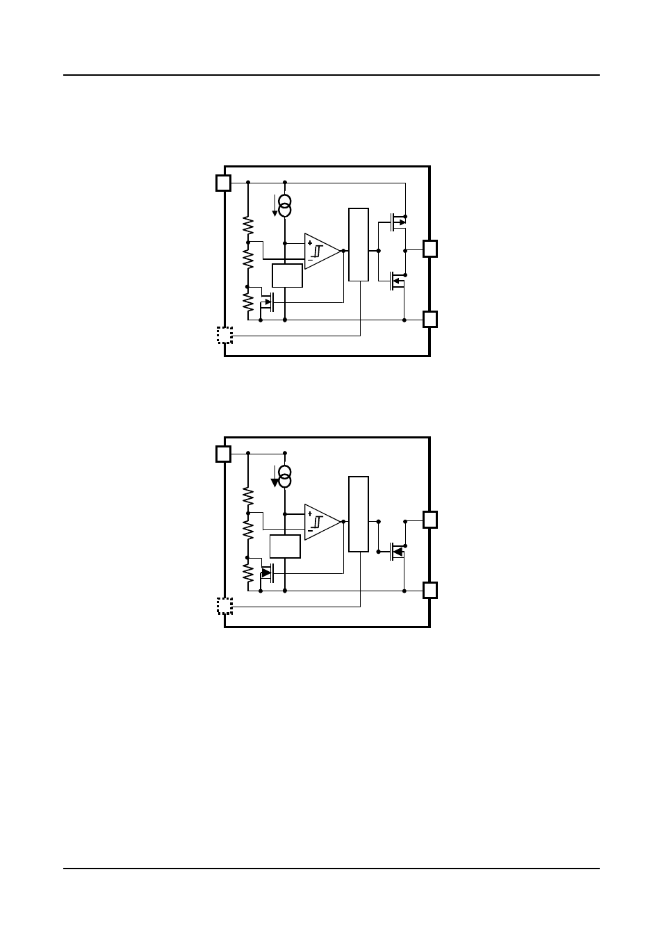
5. BLOCK DIAGRAM
2
EPSON
S1F77B01 Technical Manual (Rev.1.3)
5. BLOCK DIAGRAM
zCMOS output
zNch open drain output
Note: SOT23 package product only; otherwise, a product with DS pin set to NC
The DS pin must be fixed to “LOW” outside the IC.
V
OUT
V
DD
V
SS
D
elay circuit
V
REF
DS*
V
OUT
V
DD
V
SS
D
elay circuit
V
REF
DS*