Characteristic measuring circuits – Epson S1F77B01 User Manual
Page 15
14. CHARACTERISTIC MEASURING CIRCUITS
S1F77B01 Technical Manual (Rev.1.3)
EPSON
11
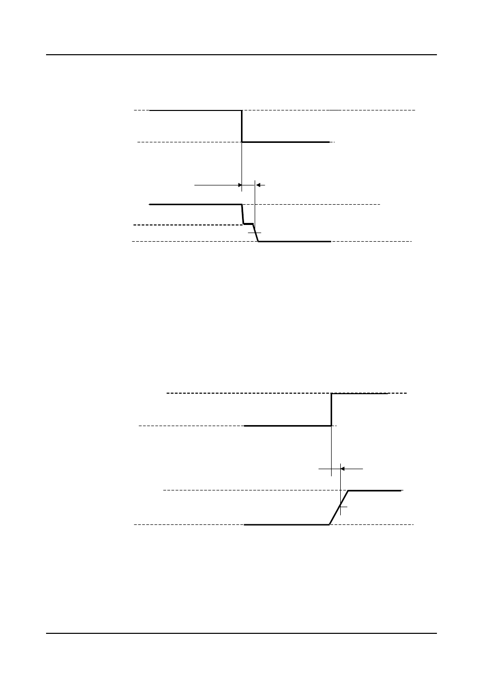
zDescription of
t
PHL
*3: V
DET
+ indicates the actual release voltage. V
DET
+=V
DET
-×1.05 (Typ.)
(1) For CMOS output
t
PHL
provides the timeframe ranging from a time when the pulse voltage (V
DET
+)+1.0V
→ 0.9V is
applied to V
DD
, to a time when the output voltage reaches V
DD
/2.
(2) Nch open drain output
t
PHL
provides the timeframe ranging from a time when the pulse voltage (V
DET
+)+1.0V
→ 0.9V is
applied to V
DD
, to a time when the output voltage reaches V
DD
/2.
The output pin is pulled up with 470k
Ω resistance and V
DD
power for measurement.
zDescription of
t
d
(1) For CMOS output
t
d provides the timeframe ranging from a time when the pulse voltage 0.9V
→ (V
DET
+)+1.0V is
applied to V
DD
, to a time when the output voltage reaches V
DD
/2.
(2) For Nch open drain output
t
d provides the timeframe ranging from a time when the pulse voltage 0.9V
→ (V
DET
+)+1.0V is
applied to V
DD
, to a time when the output voltage reaches V
DD
/2.
The output pin is pulled up with 470k
Ω resistance and V
DD
power for measurement.
50%
t
PHL
V
DD
=0.9V
Input: V
DD
Output:
V
OUT
V
OUT
=V
DD
(0.9V)
V
SS
V
DD
=V
DET
+ +1.0V
V
DD
=V
DET
+
+1.0V
*3
50%
V
DD
=V
DET
+ +1.0V
V
DD
=0.9V
Input: V
DD
Output:
V
OUT
V
OUT
= 100 %
V
SS
t
d